Community project
AI-Driven Energy Harvester Booster
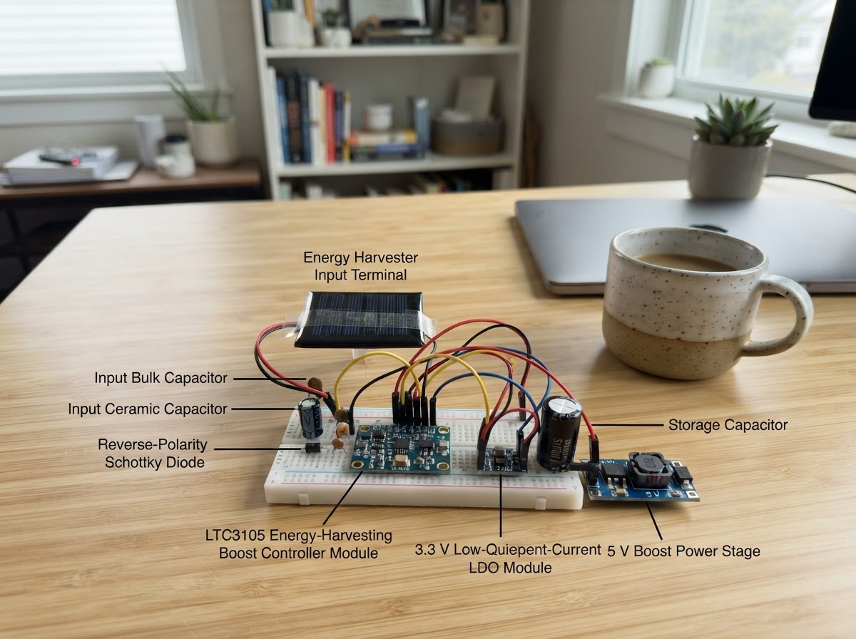
This project builds an intelligent energy harvesting system that captures power from low-voltage sources and boosts it to usable levels under ESP32 control. The system combines an LTC3105 energy-harvesting controller with a separate 5 V boost stage, gate-drive circuitry, dual current monitoring, and thermal sensing to safely extract maximum power from minimal input while protecting against overtemperature conditions.
The guide provides a complete wiring diagram, full parts list with component values, Arduino firmware with real-time sensor monitoring and OLED display output, and step-by-step assembly instructions covering cold-start circuit preparation, power rail construction, boost stage integration, and safety inspection procedures before first power-up.
Wiring diagram

Gather all the parts
Assemble it in 7 steps
1. Prepare the low-voltage source safely
Keep harvester_input disconnected while assembling. Use a solar cell or an appropriately rectified and clamped piezo source rated 0.3–1.0 V. Connect its positive lead to harvester_input VIN+ and its return to harvester_input VIN−. Connect VIN+ through reverse_diode anode A; its cathode K is the protected VIN net. Observe diode polarity: the banded cathode faces protected VIN.
- At 0.3 V, diode forward drop can prevent useful startup. Select an extremely low-VF protection part or use a designed ideal-diode circuit after engineering review.
- For a piezo source, fit a bridge rectifier and voltage clamp outside this input before connecting it.
- Never connect a bench 5 V supply directly to harvester_input: it bypasses the stated 0.3–1 V design envelope.
- A piezoelectric harvester can produce high open-circuit voltages; clamp it before this circuit.
2. Build the cold-start and 3.3 V control rail
Across protected VIN and GND, fit cin_bulk with its positive lead to VIN and negative striped lead to GND, then fit cin_ceramic in parallel. Connect cold_start VIN to VIN and GND to GND. Connect cold_start VSTORE to storage_cap positive and then to ldo_3v3 VIN; connect storage_cap negative and ldo_3v3 GND to GND. Connect ldo_3v3 VOUT to the 3.3 V rail. Connect cold_start PGOOD to ESP32 GPIO27.
- Place cin_ceramic close to cold_start VIN/GND and storage_cap close to the cold-start module.
- Configure the LTC3105 module’s MPPC/cold-start network exactly for the actual harvester, using its reference design before applying input power.
- Do not power an ESP32 DevKit from an under-rated 3.3 V LDO; ldo_3v3 must supply at least 500 mA peak with suitable local decoupling.
- Confirm VSTORE and LDO input/output voltage ratings before energizing.
3. Assemble the separate 5 V boost power stage
Build boost_stage as specified: L1 22 µH from the input rail to SW; AO3400 Q1 drain to SW, source to GND; SS34 D1 anode to SW and banded cathode to VOUT; 220 µF Cout electrolytic and 10 µF ceramic from VOUT to GND; 500 mA PTC in the outgoing VOUT path; and a 5.6 V clamp across output after the PTC. Connect boost_stage VIN to ina_input VIN− and its VOUT to ina_output VIN+. Keep all power grounds common.
- Keep the L1–Q1–D1–Cout loop physically small with short, wide conductors. Keep sensor and ESP32 wiring away from SW.
- Fit the 100 kΩ gate pulldown from Q1 gate to source and the 10 Ω series resistor between gate-driver output and Q1 gate, as stated in boost_stage.
- This discrete PWM boost stage has no proven current-limit or feedback compensation in the supplied topology. Do not energize it or enable PWM until its inductor saturation current, MOSFET/diode ratings, output clamp, and control loop have been bench-characterized.
- The 5.6 V clamp is emergency protection, not a regulation method. It can overheat if the converter is uncontrolled.
4. Wire gate drive and ESP32 control pins
Connect gate_driver VDD to the protected 5 V rail and GND to common ground. Connect gate_driver IN to ESP32 GPIO25 (PWM_GATE), and OUT through the 10 Ω gate resistor to boost_stage GATE/Q1 gate. Connect boost_stage EN to ESP32 GPIO26. Use ESP32 GPIO27 only for cold_start PGOOD. Do not use boot-strapping GPIO0, 2, 5, 12, or 15 for these signals.
- Verify that the exact gate-driver module accepts a 3.3 V HIGH input at its selected VDD before use.
- The supplied firmware intentionally keeps the PWM and boost enable off.
- Do not connect the gate-driver output directly to an ESP32 pin; the driver output is a 5 V signal intended only for Q1’s gate network.
- All modules must share GND for valid PWM and I2C signaling.
5. Wire the 3.3 V sensing and display bus
Connect VCC and GND of ina_input, ina_output, temp_sensor, and oled to the 3.3 V and GND rails. Make a shared SDA net from ESP32 GPIO21 to both INA219 SDA pins and oled SDA. Make a shared SCL net from ESP32 GPIO22 to both INA219 SCL pins and oled SCL. Set the input INA219 to address 0x40 and output INA219 to 0x41 using their module address jumpers. Connect temp_sensor DATA to ESP32 GPIO4 and fit a 4.7 kΩ resistor from DATA to 3.3 V. Thermally bond the DS18B20 body to Q1 without shorting its leads.
- Power all I2C modules at 3.3 V so their pull-ups do not drive ESP32 pins above 3.3 V.
- Keep the INA219 shunt connections as Kelvin-style short pairs where practical.
- A 0.1 Ω shunt drops 50 mV and dissipates 25 mW at 500 mA; verify this loss is tolerable on the ultra-low input rail and use a suitably rated shunt.
- Do not let an OLED or INA219 breakout pull SDA/SCL up to 5 V.
6. Connect output, charger, and battery correctly
Connect ina_output VIN− to the protected 5 V rail. Connect load_header VOUT to that 5 V rail and its GND to common ground. Connect charger IN+ to protected 5 V and IN− to GND. Connect charger B+ to battery +V and charger B− to battery GND, observing cell polarity. Connect charger OUT+ and OUT− only to battery_output_header, which is the protected 3.0–4.2 V battery output.
- Set the TP4056 charge current below the sustained available harvester output. Typical 1 A TP4056 modules are unsuitable for tiny harvesters without resistor modification.
- Use a protected 18650 cell in a proper insulated holder.
- Never connect the TP4056 protected battery output (battery_output_header) directly to the 5 V output. A proper power-path/boost design is required if the battery must power the 5 V load.
- The fitted load_header is 5 V only; do not attach a 12 V load.
7. Inspect before first power
With no battery and no harvester connected, check for shorts between VIN/GND, 3.3 V/GND, and 5 V/GND. Confirm all electrolytic capacitor polarities, SS34 and reverse_diode bands, MOSFET pinout for the actual AO3400 package, and every module’s GND. First test only the cold-start/3.3 V path with a current-limited source appropriate to cold_start. The monitoring firmware may then be deployed with Schematik’s Deploy button; it starts with boost PWM disabled.
- Measure 3.3 V at the ESP32 rail before attaching the ESP32 and confirm I2C addresses with a scan if a device is absent.
- Use an oscilloscope and current-limited source before authorizing any boost-stage PWM development.
- Do not insert the 18650 backward or work on the circuit with the cell connected.
- The submitted firmware is a safe monitoring baseline, not a closed-loop MPPT controller; it intentionally cannot turn the power stage on.
Review all connections
1. Connections between "harvester_input" and "ESP32"
2. Connections between "reverse_diode" and "ESP32"
3. Connections between "cin_bulk" and "ESP32"
4. Connections between "cin_ceramic" and "ESP32"
5. Connections between "cold_start" and "ESP32"
6. Connections between "storage_cap" and "ESP32"
7. Connections between "ldo_3v3" and "ESP32"
8. Connections between "ina_input" and "ESP32"
9. Connections between "boost_stage" and "ESP32"
10. Connections between "gate_driver" and "ESP32"
11. Connections between "ina_output" and "ESP32"
12. Connections between "temp_sensor" and "ESP32"
13. Connections between "oled" and "ESP32"
14. Connections between "charger" and "ESP32"
15. Connections between "load_header" and "ESP32"
Deploy the firmware
#include <Arduino.h>
#include <Wire.h>
#include <Adafruit_INA219.h>
#include <OneWire.h>
#include <DallasTemperature.h>
#include <Adafruit_GFX.h>
#include <Adafruit_SSD1306.h>


// Forward declarations
void setBoostEnabled(bool enabled);
void readSensors();
void updateDisplay();

constexpr int SDA_PIN = 21;
constexpr int SCL_PIN = 22;
constexpr int PWM_GATE_PIN = 25;
constexpr int BOOST_ENABLE_PIN = 26;
constexpr int PGOOD_PIN = 27;
constexpr int ONE_WIRE_PIN = 4;
constexpr uint8_t OLED_ADDR = 0x3C;
constexpr uint8_t INA_INPUT_ADDR = 0x40;
constexpr uint8_t INA_OUTPUT_ADDR = 0x41;
constexpr uint32_t PWM_FREQUENCY_HZ = 20000;
constexpr uint8_t PWM_RESOLUTION_BITS = 10;
constexpr uint16_t PWM_SAFE_DUTY = 0;
constexpr float OVER_TEMP_C = 80.0f;
constexpr uint32_t DISPLAY_INTERVAL_MS = 1000;

Adafruit_INA219 inaInput(INA_INPUT_ADDR);
Adafruit_INA219 inaOutput(INA_OUTPUT_ADDR);
OneWire oneWire(ONE_WIRE_PIN);
DallasTemperature temperatureBus(&oneWire);
Adafruit_SSD1306 display(128, 64, &Wire, -1);

bool inputMonitorOk = false;
bool outputMonitorOk = false;
bool displayOk = false;
bool powerGood = false;
float mosfetTemperatureC = NAN;
float inputVoltageV = NAN;
float inputCurrentMa = NAN;
float outputVoltageV = NAN;
float outputCurrentMa = NAN;
uint32_t lastDisplayMs = 0;

void setBoostEnabled(bool enabled) {
  digitalWrite(BOOST_ENABLE_PIN, enabled ? HIGH : LOW);
  ledcWrite(PWM_GATE_PIN, enabled ? PWM_SAFE_DUTY : 0);
}

void readSensors() {
  temperatureBus.requestTemperatures();
  const float temperature = temperatureBus.getTempCByIndex(0);
  mosfetTemperatureC = (temperature == DEVICE_DISCONNECTED_C) ? NAN : temperature;

  if (inputMonitorOk) {
    inputVoltageV = inaInput.getBusVoltage_V();
    inputCurrentMa = inaInput.getCurrent_mA();
  }
  if (outputMonitorOk) {
    outputVoltageV = inaOutput.getBusVoltage_V();
    outputCurrentMa = inaOutput.getCurrent_mA();
  }
}

void updateDisplay() {
  if (!displayOk || millis() - lastDisplayMs < DISPLAY_INTERVAL_MS) return;
  lastDisplayMs = millis();

  display.clearDisplay();
  display.setTextColor(SSD1306_WHITE);
  display.setTextSize(1);
  display.setCursor(0, 0);
  display.println("Harvester monitor");
  display.printf("PGOOD: %s  PWM: OFF\n", powerGood ? "YES" : "NO");
  display.printf("Vin: %.3f V %.1f mA\n", inputVoltageV, inputCurrentMa);
  display.printf("Vout: %.3f V %.1f mA\n", outputVoltageV, outputCurrentMa);
  if (isnan(mosfetTemperatureC)) {
    display.println("Q1 temp: sensor absent");
  } else {
    display.printf("Q1 temp: %.1f C\n", mosfetTemperatureC);
  }
  display.println("Tune MPPT after test");
  display.display();
}

void setup() {
  pinMode(BOOST_ENABLE_PIN, OUTPUT);
  pinMode(PGOOD_PIN, INPUT);
  ledcAttach(PWM_GATE_PIN, PWM_FREQUENCY_HZ, PWM_RESOLUTION_BITS);
  setBoostEnabled(false);

  Wire.begin(SDA_PIN, SCL_PIN);
  inputMonitorOk = inaInput.begin();
  outputMonitorOk = inaOutput.begin();
  temperatureBus.begin();
  displayOk = display.begin(SSD1306_SWITCHCAPVCC, OLED_ADDR);

  if (displayOk) {
    display.clearDisplay();
    display.setTextColor(SSD1306_WHITE);
    display.setTextSize(1);
    display.setCursor(0, 0);
    display.println("Safe startup");
    display.println("PWM disabled");
    display.display();
  }
}

void loop() {
  powerGood = digitalRead(PGOOD_PIN) == HIGH;
  readSensors();

  // This board deliberately does not enable the discrete boost stage.
  // A 0.3–1 V source, PWM duty, current limit, inductor saturation limit,
  // and compensation must be characterized on hardware before closed-loop MPPT.
  const bool thermalFault = !isnan(mosfetTemperatureC) && mosfetTemperatureC >= OVER_TEMP_C;
  setBoostEnabled(false || thermalFault);
  updateDisplay();
  delay(250);
}
Remix this project
Make it yours in one click
Open a full copy of this project in your own Schematik workspace — diagram, code, parts, and assembly steps included. Swap the sensor, add features, or redesign the whole thing with AI. The author's original stays untouched.