Community project
An Analog Circuit Class-a Guitar Pedal Thats Cor
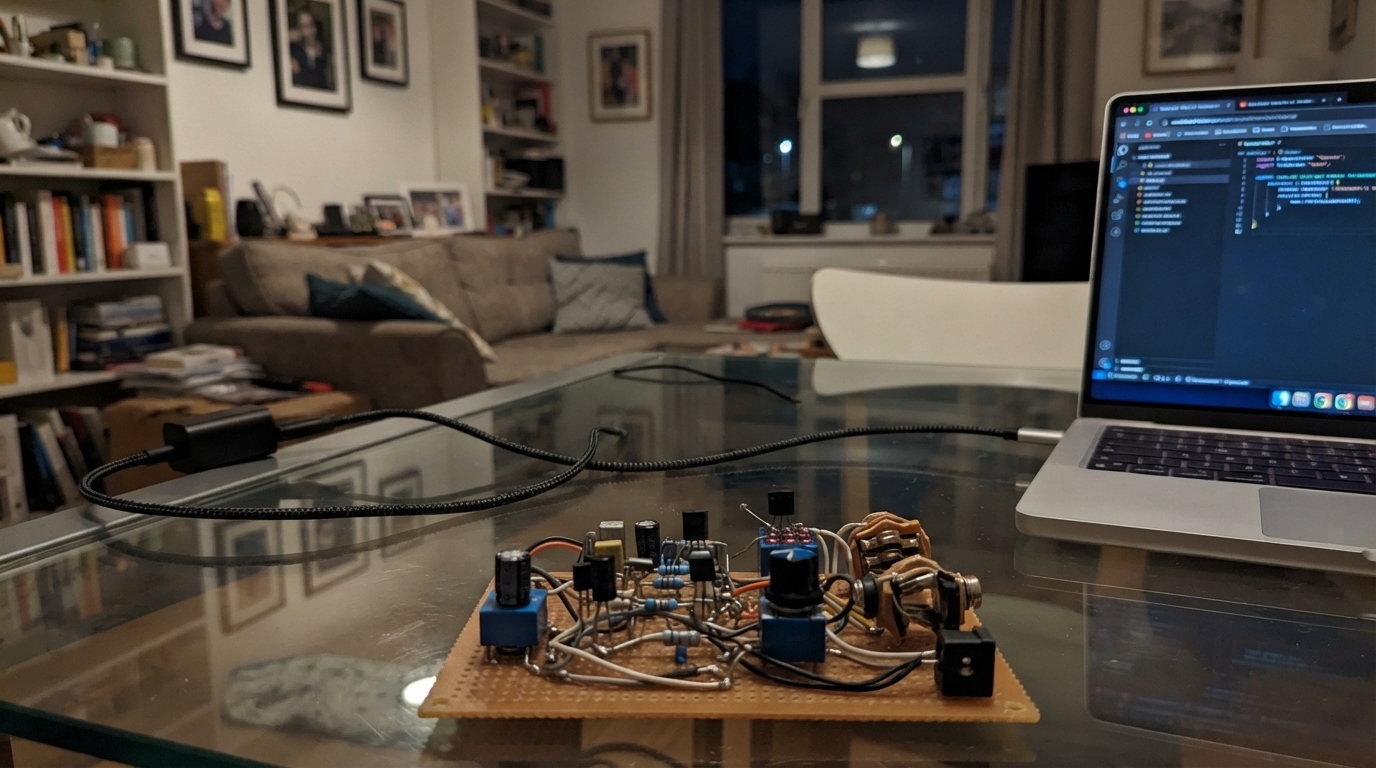
This project builds a Class-A analog guitar boost pedal with a character control that shapes the tone while increasing output level. The pedal features an external SEND/RETURN loop for inserting additional effects, all powered by a regulated boost-buck converter that accepts 9–18 V input. The circuit uses a single 2N3904 transistor in a carefully biased configuration to deliver smooth, natural amplification without digital processing.
The guide provides a complete wiring diagram, full parts list with sourcing guidance, and step-by-step assembly instructions covering power protection, audio signal routing, and final testing procedures. Builders will learn how Class-A amplification works in practice, how to implement a true bypass loop, and techniques for integrating protection circuits that prevent damage from reversed polarity or incorrect voltage supplies.
Wiring diagram

Gather all the parts
Assemble it in 6 steps
1. Mount the controls and four audio jacks
Fit the INPUT, OUTPUT, SEND, and switched RETURN quarter-inch jacks, DC jack, 3PDT footswitch, red LED, Gain control, Volume control, and Clean/Vintage toggle into the stompbox enclosure. Label SEND as “to external effect input” and RETURN as “from external effect output.”
- Use an isolated plastic jack or insulating washers if the enclosure is metal and your grounding layout requires the jack sleeves not to touch the case.
- A switched RETURN jack has a third signal lug: identify its normally-closed tip lug with the jack datasheet or a continuity meter before soldering.
- Do not confuse SEND and RETURN: SEND feeds an external effect, while RETURN receives its output.
- Do not let metal jack bodies touch uninsulated circuit-board pads; that can short the audio path to the enclosure.
2. Build the protected power section
On the PCB, wire the DC jack centre contact to ground and its outer sleeve through the 150 mA resettable fuse, reverse-polarity MOSFET stage, and bulk capacitor. Feed the protected supply into the regulated 18 V converter for the audio circuit.
- Use capacitors rated 25 V or higher on every point that can see the protected input or the 18 V rail.
- Keep converter wires and the bulk capacitor close together at one edge of the PCB, away from the INPUT jack and transistor base wiring.
- Standard pedal power is centre-negative: the centre pin is ground and the outer sleeve is positive. Reversing these connections can damage the power section.
- Use only a regulated 9–18 V pedal supply rated at least 150 mA; do not use an unregulated wall adapter.
3. Wire the boost and character control
Wire the active footswitch input through the 1 kΩ RF resistor and 100 nF input capacitor to the 2N3904 base. Add the two 1 MΩ bias resistors from 18 V to the base and from the base to ground. Wire the 4.7 kΩ collector resistor from 18 V to the collector. Wire the emitter through the 1.5 kΩ resistor and Gain control to ground. Connect the 47 µF capacitor through the Clean/Vintage switch so Vintage bypasses part of the emitter resistance and adds gentle saturation.
- For a typical 2N3904 TO-92 package, viewed with the flat face toward you and leads downward, the leads are usually Emitter, Base, Collector from left to right; confirm the purchased part’s datasheet before soldering.
- Keep the input jack, 1 kΩ resistor, RF capacitor, input capacitor, and base-bias parts physically close together.
- The striped lead of the 47 µF capacitor goes to ground. A reversed electrolytic capacitor can overheat or fail.
- Do not route the converter switching wiring beside the transistor base or input-jack trace, or audible whine may result.
4. Wire the external SEND and RETURN loop
Connect the boost output capacitor to the SEND jack TIP. Connect SEND TIP to the normally-closed TIP_NC lug of the RETURN jack; this passes the boosted signal onward when RETURN is empty. Connect the RETURN jack TIP to Volume control LUG 3. Connect both SEND and RETURN sleeves to ground. To use an external effect, run a patch lead from SEND to that effect’s input and a second patch lead from the effect’s output to RETURN.
- With no plug in RETURN, the normal contact connects SEND to the Volume control path automatically.
- An external effect keeps its own power supply; these SEND and RETURN jacks carry audio only.
- Use a normally-closed switched mono RETURN jack. An ordinary mono jack will leave the pedal silent whenever no return cable is plugged in.
- Turn down the external effect and the pedal Volume before connecting a new effect to avoid a sudden loud sound.
5. Finish the output, bypass, and status light
Wire the Volume control wiper to the JFET buffer input and wire the buffer output to the active-output contact on the footswitch. Wire one pole pair of the 3PDT so the guitar input goes either to the active boost input or directly to the output jack. Wire the second pole pair so the output jack receives either the buffered active signal or the direct bypass signal. Wire the LED long lead through the 8.2 kΩ resistor to protected positive supply, and use the third switch pole to connect its short lead to ground only when the effect is on.
- Before closing the enclosure, use a continuity tester to confirm bypass connects INPUT tip directly to OUTPUT tip while the active signal is disconnected.
- At 18 V, the 8.2 kΩ resistor keeps LED current modest; if the LED is too dim, use 6.8 kΩ but do not omit the resistor.
- The LED long lead is positive and the short lead is negative; reversed LED wiring will not light.
- Keep all jack sleeve, power-return, and circuit-ground connections solid; a missing ground causes hum or silence.
6. Inspect and test without an external effect first
With power unplugged, inspect every solder joint, confirm the electrolytic capacitor polarity, and check that no bare wires can touch the enclosure. Start with Gain and Volume low. Connect a regulated pedal supply, guitar, and amplifier, leaving SEND and RETURN empty; the switched RETURN jack should keep the active signal path working. Then test the loop using two patch leads and an externally powered effect.
- Check the transistor collector DC voltage during prototype bring-up; it should sit near the middle of the 18 V rail for clean headroom.
- If the loop loses sound only when RETURN is empty, recheck the normally-closed lug on the RETURN jack.
- Never connect the pedal’s 9 V or 18 V rails to the unrelated ESP32 board shown in the workspace; it is not part of this analog pedal.
- If you smell heating, see smoke, or the fuse trips, unplug power immediately and inspect the DC jack polarity and power wiring.
Review all connections
1. Connections between "dc_in" and "ESP32"
2. Connections between "fuse1" and "ESP32"
3. Connections between "d_reverse" and "ESP32"
4. Connections between "c_power_bulk" and "ESP32"
5. Connections between "power_converter" and "ESP32"
6. Connections between "jack_input" and "ESP32"
7. Connections between "switch_bypass" and "ESP32"
8. Connections between "r_input_rf" and "ESP32"
9. Connections between "c_input_rf" and "ESP32"
10. Connections between "c_input" and "ESP32"
11. Connections between "r_bias_top" and "ESP32"
12. Connections between "r_bias_bottom" and "ESP32"
13. Connections between "r_collector" and "ESP32"
14. Connections between "q1" and "ESP32"
15. Connections between "r_emitter" and "ESP32"
16. Connections between "pot_gain" and "ESP32"
17. Connections between "c_emitter" and "ESP32"
18. Connections between "switch_voice" and "ESP32"
19. Connections between "pot_level" and "ESP32"
20. Connections between "buffer1" and "ESP32"
21. Connections between "jack_output" and "ESP32"
22. Connections between "r_led" and "ESP32"
23. Connections between "led_status" and "ESP32"
24. Connections between "c_output" and "ESP32"
25. Connections between "jack_send" and "ESP32"
26. Connections between "jack_return" and "ESP32"
Deploy the firmware
// This project is a fully analog guitar boost pedal with external SEND/RETURN jacks.
// No microcontroller is fitted; no firmware controls the audio path.
void setup() {}
void loop() {}
Remix this project
Make it yours in one click
Open a full copy of this project in your own Schematik workspace — diagram, code, parts, and assembly steps included. Swap the sensor, add features, or redesign the whole thing with AI. The author's original stays untouched.