Community project
C Th Thi T K Pcb Theo Y
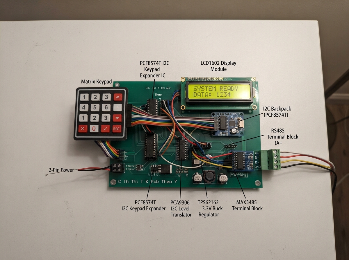
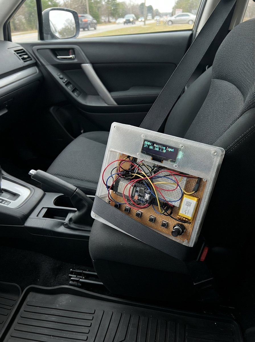
This ESP32-based control panel integrates a 4x4 matrix keypad, 16x2 LCD display, and RS485 communication on a single PCB. The keypad input is managed through an I2C expander, the display connects via I2C backpack, and RS485 enables networked communication with external devices. The design includes proper level translation between 5V and 3.3V logic domains and a regulated power supply.
This guide provides a complete wiring diagram, bill of materials, and step-by-step assembly instructions for building the PCB in KiCad. Included firmware demonstrates keypad scanning with debouncing, LCD output, and RS485 transmission, giving makers a fully functional starting point for industrial control, data entry, or remote monitoring applications.
Wiring diagram
Gather all the parts
Assemble it in 6 steps
1. Đặt khung bo hai lớp trong KiCad
Tạo board outline đúng 69,0 mm × 25,0 mm trên Edge.Cuts; dùng FR-4 hai lớp, dày 1,6 mm, đồng 1 oz và HASL chì hoặc ENIG. Dành khoảng 8 mm đầu bo cho ESP-07 và đầu U.FL anten ngoài: không đổ đồng, không đi track, không đặt via hay linh kiện dưới hoặc ngay trước vùng anten của module.
- Ghi rõ mã board và revision trên F.SilkS, ví dụ QUEUE-ESP07-R1.
- Đặt hai lỗ bắt vít M2 nếu vỏ còn đủ chỗ; giữ lỗ vít ngoài vùng anten và ngoài đường RS485.
- Đồng hoặc đường mạch sát anten làm Wi-Fi yếu và khó đoán, dù mạch vẫn có thể khởi động bình thường.
2. Vẽ khối nguồn 5 V và 3,3 V
Nối đầu vào +5V qua cầu chì tự phục hồi vào net +5V_PROT; TVS 5 V nối từ +5V_PROT xuống GND. Đặt tụ đầu vào 10 µF sát chân VIN/GND của TPS62162. Nối chân SW của TPS62162 đến cuộn cảm 2,2 µH bằng đường thật ngắn; đầu kia cuộn cảm là net +3V3, có tụ 22 µF sát GND. TPS62162DSGR là bản 3,3 V cố định; nối FB xuống AGND theo khuyến nghị datasheet hoặc để hở theo datasheet, không tự thêm cầu phân áp. Kéo EN lên VIN để nguồn luôn bật.
- Dùng trace nguồn 5 V và 3,3 V rộng ít nhất 0,5 mm; đoạn VIN–IC–GND–tụ đầu vào cần ngắn nhất có thể.
- Tạo một vùng GND gần như kín mặt đáy; khâu via GND quanh khối buck nhưng không tạo vòng đồng dưới vùng anten.
- Không kéo đường SW dài hoặc chạy dưới ESP-07, keypad hay I2C — xung chuyển mạch của buck có thể gây nhiễu.
3. Vẽ ESP-07, boot và cổng nạp
Đặt ESP-07 sát cạnh board, đầu nối U.FL hướng ra cạnh vỏ dễ gắn anten ngoài. Kéo EN, RST, GPIO0 và GPIO2 lên +3V3 bằng 10 kΩ; kéo GPIO15 xuống GND bằng 10 kΩ. RESET là nút nối RST xuống GND; FLASH là nút nối GPIO0 xuống GND. Header bảo trì theo thứ tự DTR, RXD, TXD, 3V3, RTS, GND; RXD header nối TXD/GPIO1 của ESP và TXD header nối RXD/GPIO3. Hai MMBT3904 kéo GPIO0 và RST xuống GND theo DTR/RTS qua điện trở base 10 kΩ.
- Đặt tụ 100 nF và tụ khối 10 µF gần chân cấp nguồn ESP-07.
- Đặt RESET và FLASH sát mép bo để chạm được khi bo đã nằm trong vỏ.
- Chỉ dùng USB-to-UART mức logic 3,3 V; mức 5 V tại RXD hoặc GPIO có thể hỏng ESP-07.
4. Vẽ keypad và bus LCD ngoài
Nối GPIO4/SDA và GPIO5/SCL với PCF8574T, mỗi đường có điện trở kéo lên 4,7 kΩ về +3V3. Đặt A0, A1, A2 của PCF8574T xuống GND để địa chỉ keypad là 0x20. Nối P0–P7 lần lượt đến header keypad R1, R2, R3, R4, C1, C2, C3, C4. PCA9306 có VREF1 = +3V3, VREF2 = +5V, GND chung và EN kéo lên +3V3; phía LCD của SDA/SCL được kéo lên +5V bằng 4,7 kΩ. Header LCD ghi rõ GND, +5V, SDA, SCL.
- Đặt đầu keypad và LCD sát mép bo theo hướng dây đi vào vỏ để không bị gập cáp.
- Dùng cáp LCD ngắn; với cáp dài, chọn cáp có các dây GND xen kẽ hoặc giảm tốc độ I2C trong firmware.
- Không nối trực tiếp SDA/SCL 5 V từ LCD vào GPIO4/GPIO5; bộ PCA9306 là lớp bảo vệ bắt buộc.
5. Vẽ RS485 có bảo vệ
Nối TXD/GPIO1 đến DI, RXD/GPIO3 đến RO của MAX3485; chập DE và RE rồi nối GPIO12. Đặt SM712 sát terminal A/B, sau đó đi A/B tới MAX3485 dạng cặp song song ngắn. Dùng jumper hàn SJ1 nối điện trở 120 Ω giữa A và B để chỉ đóng khi board ở đầu tuyến RS485. Đưa A, B và GND ra terminal ba chân.
- Ghi A, B, GND thật lớn trên silkscreen; thiết bị RS485 khác hãng đôi khi đổi tên A/B, nên kiểm tra thực tế khi nghiệm thu.
- Đặt terminal RS485 ở mép đối diện vùng anten và tách khỏi khối buck.
- Chỉ hàn SJ1 ở một trong hai đầu vật lý của tuyến dây RS485; đóng ở mọi nút làm tín hiệu yếu đi.
6. Kiểm tra trước khi xuất bộ hồ sơ sản xuất
Trong KiCad chạy ERC cho schematic và DRC cho PCB; tạo Net Class nguồn tối thiểu 0,5 mm, tín hiệu thông thường 0,20–0,25 mm theo khả năng xưởng. Xuất Gerber, Excellon drill, BOM, pick-and-place, PDF schematic và drawing ghi stackup hai lớp. Trước khi lắp hàng loạt, lắp 3 đến 5 board pilot rồi đo +3V3, nạp firmware và thử keypad, LCD, Wi-Fi và RS485.
- Thêm test point cho +5V_PROT, +3V3, GND, RST, GPIO0, TXD, RXD, SDA và SCL.
- Với nhà máy, gửi cả file .kicad_sch/.kicad_pcb nguồn, không chỉ Gerber, để dễ đối chiếu revision.
- Đừng đưa board vào sản xuất hàng loạt chỉ vì ERC không báo lỗi: phải đo điện áp 3,3 V và thử nạp/khởi động trên board pilot trước.
Review all connections
1. Connections between "power_input" and "ESP32"
2. Connections between "regulator_3v3" and "ESP32"
3. Connections between "keypad_expander" and "ESP32"
4. Connections between "keypad_header" and "ESP32"
5. Connections between "lcd1602_i2c" and "ESP32"
6. Connections between "lcd_header" and "ESP32"
7. Connections between "i2c_level_translator" and "ESP32"
8. Connections between "rs485" and "ESP32"
9. Connections between "rs485_terminal" and "ESP32"
10. Connections between "uart_header" and "ESP32"
11. Connections between "reset_button" and "ESP32"
12. Connections between "flash_button" and "ESP32"
13. Connections between "r_gpio0_pullup" and "ESP32"
14. Connections between "r_gpio2_pullup" and "ESP32"
15. Connections between "r_gpio15_pulldown" and "ESP32"
16. Connections between "r_i2c_sda" and "ESP32"
17. Connections between "r_i2c_scl" and "ESP32"
18. Connections between "rs485_termination" and "ESP32"
19. Connections between "decoupling_100nf" and "ESP32"
20. Connections between "bulk_caps" and "ESP32"
21. Connections between "r_en_pullup" and "ESP32"
22. Connections between "r_rst_pullup" and "ESP32"
23. Connections between "q_flash_auto" and "ESP32"
24. Connections between "q_reset_auto" and "ESP32"
25. Connections between "rst_cap" and "ESP32"
26. Connections between "input_fuse" and "ESP32"
27. Connections between "input_tvs" and "ESP32"
28. Connections between "buck_inductor" and "ESP32"
29. Connections between "buck_input_cap" and "ESP32"
30. Connections between "buck_output_cap" and "ESP32"
31. Connections between "rs485_tvs" and "ESP32"
32. Connections between "i2c_lcd_pullups" and "ESP32"
Deploy the firmware
#include <Arduino.h>
#include <Wire.h>
#include <LiquidCrystal_I2C.h>


// Forward declarations
void pcfWrite(uint8_t value);
uint8_t pcfRead();
char scanKeypad();
void showKey(char key);
void sendKeyToRs485(char key);
void handleAcceptedKey(char key);

constexpr uint8_t I2C_SDA_PIN = 4;
constexpr uint8_t I2C_SCL_PIN = 5;
constexpr uint8_t RS485_DIR_PIN = 12;
constexpr uint8_t KEYPAD_PCF8574_ADDRESS = 0x20;
constexpr uint8_t LCD_I2C_ADDRESS = 0x27;
constexpr unsigned long DEBOUNCE_MS = 35;

LiquidCrystal_I2C lcd(LCD_I2C_ADDRESS, 16, 2);

const char KEYMAP[4][4] = {
  {'1', '2', '3', 'A'},
  {'4', '5', '6', 'B'},
  {'7', '8', '9', 'C'},
  {'*', '0', '#', 'D'}
};

char lastRawKey = '\0';
char acceptedKey = '\0';
unsigned long rawKeyChangedAt = 0;

void pcfWrite(uint8_t value) {
  Wire.beginTransmission(KEYPAD_PCF8574_ADDRESS);
  Wire.write(value);
  Wire.endTransmission();
}

uint8_t pcfRead() {
  Wire.requestFrom(static_cast<int>(KEYPAD_PCF8574_ADDRESS), 1);
  return Wire.available() ? static_cast<uint8_t>(Wire.read()) : 0xFF;
}

char scanKeypad() {
  for (uint8_t row = 0; row < 4; ++row) {
    // P0..P3 are rows. One row is driven low; P4..P7 remain released as inputs.
    uint8_t rowPattern = static_cast<uint8_t>(0xF0 | (0x0F & ~(1U << row)));
    pcfWrite(rowPattern);
    delayMicroseconds(80);
    uint8_t sample = pcfRead();

    for (uint8_t column = 0; column < 4; ++column) {
      if ((sample & (1U << (column + 4))) == 0) {
        pcfWrite(0xFF);
        return KEYMAP[row][column];
      }
    }
  }
  pcfWrite(0xFF);
  return '\0';
}

void showKey(char key) {
  lcd.setCursor(0, 1);
  lcd.print("Key: ");
  lcd.print(key);
  lcd.print("          ");
}

void sendKeyToRs485(char key) {
  digitalWrite(RS485_DIR_PIN, HIGH);
  delayMicroseconds(20);
  Serial.print("KEY,");
  Serial.println(key);
  Serial.flush();
  delayMicroseconds(20);
  digitalWrite(RS485_DIR_PIN, LOW);
}

void handleAcceptedKey(char key) {
  showKey(key);
  sendKeyToRs485(key);
}

void setup() {
  pinMode(RS485_DIR_PIN, OUTPUT);
  digitalWrite(RS485_DIR_PIN, LOW);  // Receive mode after power-up.

  Serial.begin(9600);
  Wire.begin(I2C_SDA_PIN, I2C_SCL_PIN);
  Wire.setClock(100000);
  pcfWrite(0xFF);

  lcd.init();
  lcd.backlight();
  lcd.setCursor(0, 0);
  lcd.print("Queue terminal");
  lcd.setCursor(0, 1);
  lcd.print("Ready           ");
}

void loop() {
  char rawKey = scanKeypad();
  unsigned long now = millis();

  if (rawKey != lastRawKey) {
    lastRawKey = rawKey;
    rawKeyChangedAt = now;
  }

  if ((now - rawKeyChangedAt) >= DEBOUNCE_MS && rawKey != acceptedKey) {
    acceptedKey = rawKey;
    if (acceptedKey != '\0') {
      handleAcceptedKey(acceptedKey);
    }
  }
}
Remix this project
Make it yours in one click
Open a full copy of this project in your own Schematik workspace — diagram, code, parts, and assembly steps included. Swap the sensor, add features, or redesign the whole thing with AI. The author's original stays untouched.