Community project
Multi-Rail Battery Power Board
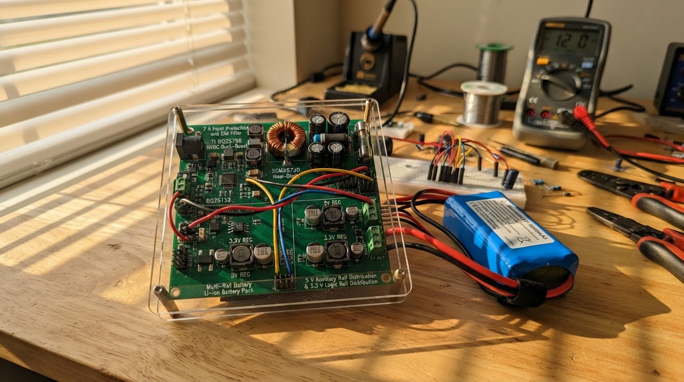
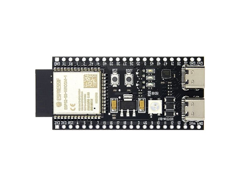
This multi-rail battery power board delivers regulated 5 V and 3.3 V outputs from a 12 V Li-ion battery pack, with integrated charging and reverse-polarity protection. The TI BQ25798 buck-boost charger manages input power and battery state, while dual buck converters supply independent rails for logic and auxiliary loads. An ESP32-S3 controller monitors charging status, input presence, and power-path behavior via I2C and GPIO signals.
Builders will receive a complete wiring diagram, detailed parts list, validated firmware for the external controller, and step-by-step assembly instructions including pre-power inspection, battery connection, and safe bring-up procedures. The guide covers safe telemetry integration, incremental load validation, and the role of hardware protection versus software monitoring in fault containment.
Wiring diagram

Gather all the parts
Assemble it in 7 steps
1. Prepare the board and the external controller
Place the UPS power board and the separately powered ESP32-S3 controller on a non-conductive bench. Do not connect J1 input, J2A battery, or J3 loads while inspecting the assembly.
- Confirm that J3 is the Molex Micro-Fit 3.0 2×3 footprint selected for this revision, not a generic 2.54 mm header.
- The header orientation must match the frozen header-face pin numbering in data/POWER_PATH_LAYOUT_REVISION_R1.md.
- Never connect mains AC to J1.
- This project record is not proof that an untested prototype is safe to energize.
2. Build the J3 mating harness
Use the matching Micro-Fit 3.0 receptacle housing and compatible female terminals with 20 AWG stranded 105 °C wire. Terminate one conductor to each used contact; do not rely on a solder bridge or a single wire to create the paired SYS or ground paths.
- Header-face mapping: pin 1 SYS_BUS_A, pin 2 SYS_BUS_B, pin 3 GND_A, pin 4 GND_B, pin 5 5V0_OUT, pin 6 3V3_OUT.
- Keep the paired SYS wires equal in gauge and approximately equal in length; do the same for paired grounds.
- Do not reverse the header-face view with the cable-entry view.
- Do not parallel contacts with unequal or undersized harness wiring; uneven resistance can overload one contact.
3. Inspect high-current board paths before power
Inspect the BQ25798 SYS_BUS route, J3 pins 1–4 pours, battery path, 5 V and 3.3 V buck layouts, and all high-current vias for solder bridges, damage, or unintended narrow neck-downs.
- The preliminary layout rules and validation limits are recorded in data/POWER_PATH_LAYOUT_REVISION_R1.md.
- Check that the two SYS contacts and two ground contacts have symmetric copper geometry.
- Do not assume a nominal BMS rating or a controller reboot protects a defective PCB path.
- Do not perform a short-circuit test until the exact BQ25798 and BMS response has been verified and a reviewed fault fixture is available.
4. Connect the battery and NTC harness
With all external power absent, connect the protected 3S battery pack to J2A with PACK+ to BAT+ and PACK− to BAT−. Connect the pack NTC harness to J2B only if it is the intended 10 kΩ battery thermistor.
- The intended battery is 3S1P Li-ion: 11.1 V nominal and 12.6 V maximum.
- Verify battery polarity with a meter before mating the connector.
- Reverse battery polarity or an incompatible pack can damage the board.
- Do not use battery voltage as a precise state-of-charge measurement without validation.
5. Connect low-voltage telemetry safely
Connect J10 between the UPS board and the external ESP32-S3 controller using the documented 3.3 V logic signals and common ground. Keep the controller USB connection separate from high-current J3 wiring.
- J10 is a 3.3 V interface; do not apply 5 V, SYS_BUS, or external power to its signal pins.
- Confirm the controller is not back-powering the UPS board before normal testing.
- Unplugged-controller and USB-backfeed behavior remain validation items.
6. Bring up with a compliant regulated DC source
Connect only a regulated 12 V or 24 V DC source within the documented 10.8–24.0 V normal J1 range. Begin with current-limited bench power and no J3 load, then observe the rail test points.
- Use TP1/TP2 for input domain checks, TP3 for SYS_BUS, TP4 for 5 V, TP5 for 3.3 V, and TP6 for ground reference.
- The nominal 26 V input eFuse threshold is an abnormal-fault disconnect, not permission to operate normally above 24.0 V.
- Never connect AC mains directly to J1.
- Do not energize a board with visible damage, unknown battery polarity, or unreviewed wiring.
7. Validate loads incrementally
After no-load rail checks, add controlled loads one at a time. Test J3 SYS_BUS, 5V0_OUT, and 3V3_OUT separately before attempting combined loading or power-cutover tests.
- Follow the staged controlled-load and thermal procedure in data/POWER_PATH_LAYOUT_REVISION_R1.md.
- Use thermal monitoring during sustained-current tests and document measurements.
- A dead short is not a first bring-up test and must not be made using loose wire.
- No claimed BQ25798 short response, BMS trip timing, or buck hiccup behavior is accepted until verified on the exact design.
Review all connections
1. Connections between "j1_field_terminal" and "ESP32"
2. Connections between "input_protection_1" and "ESP32"
3. Connections between "ideal_diode_1" and "ESP32"
4. Connections between "battery_3s_1" and "ESP32"
5. Connections between "j2a_battery" and "ESP32"
6. Connections between "j2b_ntc" and "ESP32"
7. Connections between "bq25798_1" and "ESP32"
8. Connections between "j10_interface_protection_1" and "ESP32"
9. Connections between "buck_5v_1" and "ESP32"
10. Connections between "rail_5v_output_1" and "ESP32"
11. Connections between "buck_logic_1" and "ESP32"
12. Connections between "rail_logic_output_1" and "ESP32"
13. Connections between "j3_distribution" and "ESP32"
14. Connections between "led_r_vin_1" and "ESP32"
15. Connections between "led_r_sys_1" and "ESP32"
16. Connections between "led_r_5v_1" and "ESP32"
17. Connections between "led_r_3v3_1" and "ESP32"
18. Connections between "diagnostic_leds_1" and "ESP32"
19. Connections between "pca9515a_1" and "ESP32"
20. Connections between "mains_good_1" and "ESP32"
21. Connections between "qon_storage_1" and "ESP32"
22. Connections between "wake_button_1" and "ESP32"
23. Connections between "input_efuse_1" and "ESP32"
24. Connections between "j10_telemetry" and "ESP32"
Deploy the firmware
/*
  External ESP32-S3 controller for the direct-input 3S UPS Power Board.
  J10: 3.3 V, GND, buffered SDA/SCL, BQ_INT, BQ_STAT, BQ_CE,
  active-low MAINS_GOOD, and protected QON_CMD.

  The controller is not a safety mechanism. Hardware protection, BMS limits,
  and validated power-path behavior remain responsible for fault containment.
*/
#include <Arduino.h>
#include <Wire.h>


// Forward declarations
void IRAM_ATTR onMainsGoodChange();
void requestQonWake();

constexpr int I2C_SDA_PIN = 8;
constexpr int I2C_SCL_PIN = 9;
constexpr int BQ_INT_PIN = 4;
constexpr int BQ_STAT_PIN = 5;
constexpr int BQ_CE_PIN = 6;
constexpr int MAINS_GOOD_PIN = 7;
constexpr int QON_CMD_PIN = 14;

volatile bool inputStateChanged = false;
volatile bool fieldInputPresent = false;

void IRAM_ATTR onMainsGoodChange() {
  // J10 MAINS_GOOD is active low when qualified external DC is present.
  fieldInputPresent = (digitalRead(MAINS_GOOD_PIN) == LOW);
  inputStateChanged = true;
}

void requestQonWake() {
  // Verify QON polarity, pulse width, and allowed state transitions against
  // the final validated BQ25798 circuit. This is intentionally manual only.
  digitalWrite(QON_CMD_PIN, LOW);
  delay(100);
  digitalWrite(QON_CMD_PIN, HIGH);
}

void setup() {
  Serial.begin(115200);
  Wire.begin(I2C_SDA_PIN, I2C_SCL_PIN);

  // Pull-ups and signal protection are on the UPS board. Do not enable ESP32
  // internal pull-ups, which could back-power an unpowered UPS board.
  pinMode(BQ_INT_PIN, INPUT);
  pinMode(BQ_STAT_PIN, INPUT);

  // Keep charge-enable high impedance. Its final pull network and polarity
  // must follow the released BQ25798 reference design before firmware drives it.
  pinMode(BQ_CE_PIN, INPUT);

  pinMode(MAINS_GOOD_PIN, INPUT);
  fieldInputPresent = (digitalRead(MAINS_GOOD_PIN) == LOW);
  attachInterrupt(digitalPinToInterrupt(MAINS_GOOD_PIN), onMainsGoodChange, CHANGE);

  // The protection stage defines the inactive QON state as high.
  pinMode(QON_CMD_PIN, OUTPUT);
  digitalWrite(QON_CMD_PIN, HIGH);

  Serial.println("UPS controller ready. Send w for a manual QON wake pulse.");
}

void loop() {
  if (inputStateChanged) {
    noInterrupts();
    const bool present = fieldInputPresent;
    inputStateChanged = false;
    interrupts();

    Serial.println(present
      ? "Field input qualified present"
      : "Field input lost; shed nonessential controller loads now.");
  }

  if (Serial.available() && Serial.read() == 'w') {
    requestQonWake();
    Serial.println("Manual QON wake pulse requested.");
  }

  static uint32_t lastReportMs = 0;
  if (millis() - lastReportMs >= 1000) {
    lastReportMs = millis();
    Serial.print("MAINS_GOOD=");
    Serial.print(fieldInputPresent ? "present" : "absent");
    Serial.print(" BQ_INT=");
    Serial.print(digitalRead(BQ_INT_PIN) == LOW ? "active" : "idle");
    Serial.print(" BQ_STAT=");
    Serial.println(digitalRead(BQ_STAT_PIN) == LOW ? "active" : "idle");
  }
}
Remix this project
Make it yours in one click
Open a full copy of this project in your own Schematik workspace — diagram, code, parts, and assembly steps included. Swap the sensor, add features, or redesign the whole thing with AI. The author's original stays untouched.