Community project
NiMH Battery Health Tester
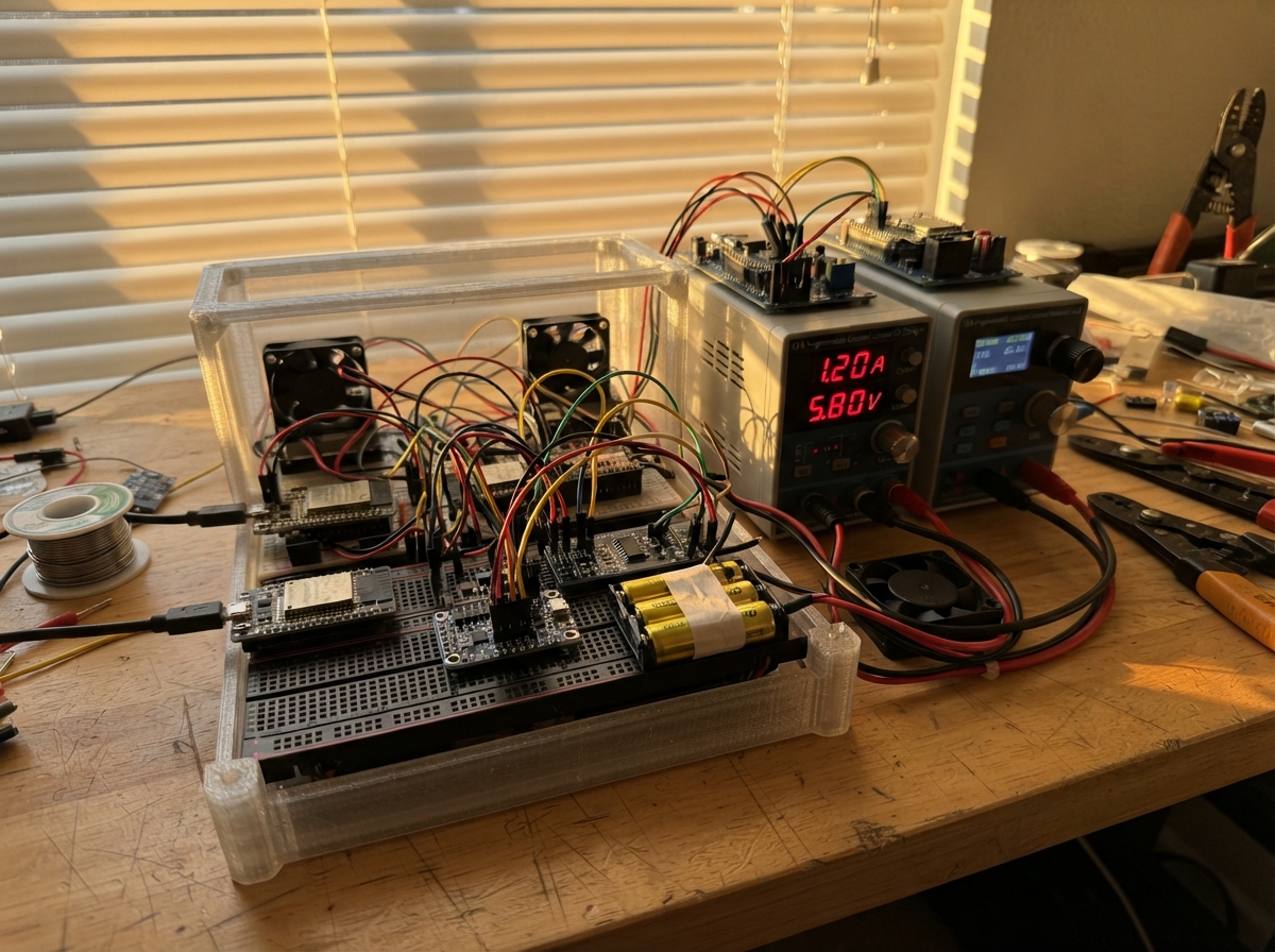
This project builds a dual-channel battery health tester for NiMH cells using two ESP32 controllers to independently monitor and stress-test 7.2 V battery modules. The system performs controlled charge and discharge cycles while measuring voltage, current, and temperature in real time, allowing makers to assess battery capacity degradation and internal resistance over multiple test runs.
The guide provides a complete wiring diagram, parts list, and step-by-step assembly instructions for mounting the high-current charging modules, connecting the dual INA237 power monitors and DS18B20 temperature sensors, and configuring the RS485 communication network between the main controller and two data acquisition nodes. Firmware is included to automate the test sequence, log results, and enforce safety interlocks throughout operation.
Wiring diagram

Gather all the parts
Assemble it in 8 steps
1. Mount the high-current equipment safely
Place the two 150 W electronic loads on a non-flammable bench with clear airflow around their heat sinks and fans. Mount the two charging stages, the 15 V laboratory supply, fuses, and the normally closed mushroom emergency-stop switch in an insulated enclosure or guarded test fixture. Keep the ESP32 boards and RS485 wiring physically away from the high-current battery cables.
- Use short, heavy battery leads sized for at least 10 A continuous current.
- Label the two channels CH1 and CH2 before connecting anything.
- The electronic loads can become hot enough to burn skin during repeated tests; do not touch their heat sinks until they cool.
- Do not use an unguarded breadboard for 5–6.5 A battery wiring; loose wires can overheat or start a fire.
2. Make the protected battery connections
For each module, fit a 10 A DC-rated fuse in the positive lead close to the battery terminal. Connect module 1 positive to current_monitor_1 VIN+ and the channel 1 protected positive bus; connect charge_stage_1 OUT+ through the monitor path and load_stage_1 IN+ to that same protected bus. Connect charge_stage_1 OUT- and load_stage_1 IN- to battery_module_1 NEG. Repeat the same arrangement for module 2 with current_monitor_2, charge_stage_2, load_stage_2, and battery_module_2. The positive lead carries the test current; the negative lead completes its return path.
- Use the same cable length and connector type on both channels for more repeatable data.
- Before connecting a module, check its open-circuit voltage with a meter and ensure the correct positive and negative terminals are identified.
- Reversing a NiMH module can damage the charger, electronic load, current monitor, or wiring.
- The INA237 monitor’s 15 mΩ shunt is only suitable when the actual board and shunt are verified for the full pulse current; do not exceed its stated current and power rating.
3. Wire the 15 V charging supply
With the laboratory supply switched off, connect supply_15v V+ to charge_stage_1 DC_IN+ and charge_stage_2 DC_IN+. Connect supply_15v V- to charge_stage_1 DC_IN- and charge_stage_2 DC_IN-. Set the supply current limit conservatively before the first powered check, then raise it only after verifying that both charger stages are off at zero command.
- A 15 V, 25 A isolated supply gives room for two 6.5 A charge pulses plus conversion losses.
- Use a separately fused branch for each charging stage.
- Do not connect the 15 V supply directly to a 7.2 V module; the regulated charging stage must be between them.
- Wrong supply polarity can damage both charging stages immediately.
4. Attach the temperature probes
Tape temp_sensor_1 firmly against the middle of module 1 using electrically insulating tape, then cover it with a small foam pad so it follows cell temperature instead of room airflow. Do the same for temp_sensor_2 on module 2. Connect each DS18B20 VCC to 3V3 (power), GND to GND (ground), and DATA to its local DAQ temperature input (signal). Fit one 4.7 kΩ resistor from each DATA wire to 3V3 so the temperature signal can return to its idle state.
- Keep each temperature sensor’s wires away from the load heat sink and high-current cables.
- Confirm that each DAQ reports a believable room-temperature value before a battery is connected.
- A loose probe can read cool air while the module overheats, defeating the temperature stop protection.
5. Wire each DAQ’s measurement and command side
For channel 1, connect current_monitor_1 VCC to 3V3 (power), GND to daq1_esp32 GND (ground), SDA to daq1_esp32 SDA (data), and SCL to daq1_esp32 SCL (clock). Connect dac_1 VCC to 3V3 (power), GND to daq1_esp32 GND (ground), SDA and SCL to the same local I2C wires, and DAC OUT to command_selector_1 IN (current command). Wire command_selector_1 CHARGE_CMD to charge_stage_1 CURRENT_CMD and LOAD_CMD to load_stage_1 CURRENT_CMD. Repeat these connections for channel 2 with the parts ending in _2. The DAC voltage is only the desired-current command; the charger or load’s own current-feedback circuit drives its MOSFET power stage and measured current toward that request.
- Calibrate DAC voltage against actual current with a trusted meter before testing batteries.
- Use the two different MCP4725 address links so each local DAQ can identify its DAC.
- Never feed battery voltage into an ESP32 GPIO, DAC pin, or I2C pin; they are low-voltage control wires only.
- Do not assume two different charger/load modules share the same command-voltage-to-current scaling; calibrate every channel.
6. Install the direction interlock and emergency stop
Connect daq1_esp32 CHARGE_EN to safety_interlock CH1_CHARGE_EN (charge request) and daq1_esp32 DISCHARGE_EN to safety_interlock CH1_LOAD_EN (discharge request). Connect the corresponding channel 2 signals to CH2 inputs. Connect the interlock outputs to each stage’s INHIBIT input and its select output to the channel command selector. Wire the mushroom switch as the normally closed E_STOP_NC loop. The interlock must force both charge and discharge enables off when the stop button opens or when opposite paths are requested.
- Test the emergency-stop switch with no battery attached: it must disable every stage immediately.
- The firmware must command zero current, wait for measured current to settle, then switch direction; the hardware interlock is the second layer of protection.
- Do not bypass the hardware interlock: charging and discharging a module through incompatible paths at the same time can destroy equipment and overheat the module.
7. Build the shared RS485 communication cable
On the main controller, connect rs485_bus VCC to 3V3 (power), GND to GND (ground), RO to GPIO16 (receive data), DI to GPIO17 (send data), DE to GPIO27 (send-enable signal), and RE to GPIO26 (receive-enable signal). Daisy-chain the A wire from rs485_bus to rs485_daq1 A to rs485_daq2 A, and similarly daisy-chain B to B. Use one twisted pair for A and B, add a 120 Ω resistor across A and B only at the two physical ends of the cable, and use a common signal reference or isolated RS485 transceivers as required by the fixture grounding arrangement.
- Label the nodes Master, DAQ 01, and DAQ 02.
- Keep the RS485 cable separate from high-current leads to reduce electrical noise.
- A and B labels vary between RS485 modules; if the bus does not communicate, compare each module’s data sheet rather than swapping wires while equipment is powered.
- Do not place a 120 Ω termination resistor at every RS485 node; only the cable ends receive termination.
8. Check the system before a live test
Power the ESP32 boards through USB first, with the 15 V supply off and no modules connected. Confirm that all stages remain inhibited, both temperature readings are sensible, and each DAQ answers at address 01 or 02. Then connect the modules, release the emergency stop, and perform a low-current calibration check before allowing the programmed 6.5 A charge pulse, 5 A discharge pulse, and 2.1667 A fifteen-minute charge hold.
- Start with the stages limited to a small current and compare each INA237 reading with an external meter.
- The main controller records timestamp, DAQ ID, voltage, current, temperature, current target, state, and status every roughly 500 ms.
- Stop immediately if a module becomes unusually warm, swells, leaks, produces odor, reports a sensor fault, or exceeds its approved test voltage.
- The voltage cutoffs in firmware are conservative starting limits; confirm them against the exact module manufacturer’s allowable charge and discharge limits before unattended operation.
Review all connections
1. Connections between "supply_15v" and "ESP32"
2. Connections between "logic_buck_daq1" and "ESP32"
3. Connections between "logic_buck_daq2" and "ESP32"
4. Connections between "charge_stage_1" and "ESP32"
5. Connections between "charge_stage_2" and "ESP32"
6. Connections between "battery_module_1" and "ESP32"
7. Connections between "battery_module_2" and "ESP32"
8. Connections between "load_mosfet_1" and "ESP32"
9. Connections between "load_shunt_1" and "ESP32"
10. Connections between "load_mosfet_2" and "ESP32"
11. Connections between "load_shunt_2" and "ESP32"
12. Connections between "load_control_1" and "ESP32"
13. Connections between "load_control_2" and "ESP32"
14. Connections between "current_monitor_1" and "ESP32"
15. Connections between "current_monitor_2" and "ESP32"
16. Connections between "temp_sensor_1" and "ESP32"
17. Connections between "temp_sensor_2" and "ESP32"
18. Connections between "onewire_pullups" and "ESP32"
19. Connections between "dac_1" and "ESP32"
20. Connections between "dac_2" and "ESP32"
21. Connections between "rs485_bus" and "ESP32"
22. Connections between "rs485_daq1" and "ESP32"
23. Connections between "rs485_daq2" and "ESP32"
24. Connections between "safety_interlock" and "ESP32"
Deploy the firmware
#include <Arduino.h>

// Main Controller (MC) firmware for one ESP32 DevKit v1.
// Flash this file to the MC. DAQ 01 and DAQ 02 use the two child sketches
// supplied separately in the project assembly record.
// RS485 protocol: MC polls @R,<address>,<CRC16> every 500 ms.

enum TestState : uint8_t { IDLE, CHARGE_PULSE, REST_AFTER_CHARGE, DISCHARGE_PULSE, REST_AFTER_DISCHARGE, CHARGE_HOLD, COMPLETE, FAULT };
enum Mode : uint8_t { MODE_OFF, MODE_CHARGE, MODE_DISCHARGE };

struct Measurement {
  uint8_t address;
  uint32_t sequence;
  float voltageV;
  float currentA;
  float temperatureC;
  uint16_t status;
  uint32_t receivedAt;
  bool valid;
};


// Forward declarations
uint16_t crc16(const uint8_t *data, size_t length);
void rs485Receive();
void rs485Send(const char *message);
Mode commandedMode();
float commandedCurrent();
void commandOne(uint8_t address, Mode mode, float currentA);
void commandAll(Mode mode, float currentA);
void stopSafely(const char *reason);
bool safe(const Measurement &m, Mode mode);
void parseMeasurement(char *line);
void commsTask(void *);
bool elapsed();
void advance();
void testTask(void *);
void safetyTask(void *);
void loggingTask(void *);

static const int RS485_RX_PIN = 16;
static const int RS485_TX_PIN = 17;
static const int RS485_DIR_PIN = 27;  // XY-017 R/T direction pin; LOW receive, HIGH send
static const uint32_t BAUD = 115200;
static const uint32_t UPDATE_MS = 500;
static const uint32_t COMMS_TIMEOUT_MS = 1500;
static const float MAX_VOLTAGE_V = 9.30f;
static const float MIN_VOLTAGE_V = 6.00f;
static const float MAX_TEMPERATURE_C = 55.0f;
static const float MAX_CHARGE_A = 6.50f;
static const float MAX_DISCHARGE_A = 5.00f;
static const uint32_t CHARGE_PULSE_MS = 10000;
static const uint32_t REST_MS = 30000;
static const uint32_t DISCHARGE_PULSE_MS = 10000;
static const uint32_t CHARGE_HOLD_MS = 15UL * 60UL * 1000UL;

Measurement daq[2] = {{1,0,0,0,0,0,0,false}, {2,0,0,0,0,0,0,false}};
volatile TestState state = IDLE;
volatile bool faultLatched = false;
uint32_t stateStartedAt = 0;
uint32_t recordSequence = 0;

uint16_t crc16(const uint8_t *data, size_t length) {
  uint16_t crc = 0xFFFF;
  for (size_t i = 0; i < length; ++i) {
    crc ^= data[i];
    for (uint8_t b = 0; b < 8; ++b) crc = (crc & 1) ? (crc >> 1) ^ 0xA001 : (crc >> 1);
  }
  return crc;
}

void rs485Receive() { digitalWrite(RS485_DIR_PIN, LOW); }
void rs485Send(const char *message) {
  digitalWrite(RS485_DIR_PIN, HIGH);
  delayMicroseconds(20);
  Serial2.print(message);
  Serial2.flush();
  delayMicroseconds(40);
  rs485Receive();
}

const char *modeName(Mode m) {
  return m == MODE_CHARGE ? "CHARGE" : (m == MODE_DISCHARGE ? "DISCHARGE" : "OFF");
}
Mode commandedMode() {
  return (state == CHARGE_PULSE || state == CHARGE_HOLD) ? MODE_CHARGE : (state == DISCHARGE_PULSE ? MODE_DISCHARGE : MODE_OFF);
}
float commandedCurrent() {
  return state == CHARGE_PULSE ? MAX_CHARGE_A : (state == DISCHARGE_PULSE ? MAX_DISCHARGE_A : (state == CHARGE_HOLD ? 2.1667f : 0.0f));
}

void commandOne(uint8_t address, Mode mode, float currentA) {
  char body[48], frame[64];
  snprintf(body, sizeof(body), "C,%u,%s,%.4f", address, modeName(mode), currentA);
  snprintf(frame, sizeof(frame), "@%s,%04X\n", body, crc16((const uint8_t *)body, strlen(body)));
  rs485Send(frame);
}
void commandAll(Mode mode, float currentA) {
  commandOne(1, mode, currentA);
  commandOne(2, mode, currentA);
}
void stopSafely(const char *reason) {
  commandAll(MODE_OFF, 0.0f);
  faultLatched = true;
  state = FAULT;
  Serial.printf("EVENT,FAULT,%lu,%s\n", millis(), reason);
}

bool safe(const Measurement &m, Mode mode) {
  if (!m.valid || millis() - m.receivedAt > COMMS_TIMEOUT_MS || m.status != 0) return false;
  if (!isfinite(m.voltageV) || !isfinite(m.currentA) || !isfinite(m.temperatureC)) return false;
  if (m.voltageV > MAX_VOLTAGE_V || m.temperatureC > MAX_TEMPERATURE_C) return false;
  if (mode == MODE_DISCHARGE && m.voltageV < MIN_VOLTAGE_V) return false;
  if (mode == MODE_CHARGE && m.currentA > MAX_CHARGE_A * 1.10f) return false;
  if (mode == MODE_DISCHARGE && fabsf(m.currentA) > MAX_DISCHARGE_A * 1.10f) return false;
  return true;
}

void parseMeasurement(char *line) {
  if (line[0] != '@') return;
  char *last = strrchr(line, ',');
  if (!last) return;
  uint16_t claimed = (uint16_t)strtoul(last + 1, nullptr, 16);
  *last = 0;
  if (crc16((const uint8_t *)(line + 1), strlen(line + 1)) != claimed) return;
  char *save = nullptr;
  char *kind = strtok_r(line + 1, ",", &save);
  char *addr = strtok_r(nullptr, ",", &save);
  char *seq = strtok_r(nullptr, ",", &save);
  char *volts = strtok_r(nullptr, ",", &save);
  char *amps = strtok_r(nullptr, ",", &save);
  char *temp = strtok_r(nullptr, ",", &save);
  char *status = strtok_r(nullptr, ",", &save);
  if (!kind || strcmp(kind,"M") || !addr || !seq || !volts || !amps || !temp || !status) return;
  int i = atoi(addr) - 1;
  if (i < 0 || i > 1) return;
  daq[i] = {(uint8_t)(i + 1), strtoul(seq,nullptr,10), strtof(volts,nullptr), strtof(amps,nullptr), strtof(temp,nullptr), (uint16_t)strtoul(status,nullptr,0), millis(), true};
}

void commsTask(void *) {
  char line[128]; size_t used = 0; uint32_t nextPoll = 0;
  for (;;) {
    while (Serial2.available()) {
      char c = (char)Serial2.read();
      if (c == '\n' || used == sizeof(line) - 1) { line[used] = 0; if (used) parseMeasurement(line); used = 0; }
      else if (c != '\r') line[used++] = c;
    }
    if ((int32_t)(millis() - nextPoll) >= 0) {
      for (uint8_t a = 1; a <= 2; ++a) { char b[12], f[28]; snprintf(b,sizeof(b),"R,%u",a); snprintf(f,sizeof(f),"@%s,%04X\n",b,crc16((const uint8_t *)b,strlen(b))); rs485Send(f); }
      nextPoll = millis() + UPDATE_MS;
    }
    vTaskDelay(pdMS_TO_TICKS(5));
  }
}

bool elapsed() {
  uint32_t e = millis() - stateStartedAt;
  return (state == CHARGE_PULSE && e >= CHARGE_PULSE_MS) || ((state == REST_AFTER_CHARGE || state == REST_AFTER_DISCHARGE) && e >= REST_MS) || (state == DISCHARGE_PULSE && e >= DISCHARGE_PULSE_MS) || (state == CHARGE_HOLD && e >= CHARGE_HOLD_MS);
}
void advance() {
  stateStartedAt = millis();
  if (state == CHARGE_PULSE) state = REST_AFTER_CHARGE;
  else if (state == REST_AFTER_CHARGE) state = DISCHARGE_PULSE;
  else if (state == DISCHARGE_PULSE) state = REST_AFTER_DISCHARGE;
  else if (state == REST_AFTER_DISCHARGE) state = CHARGE_HOLD;
  else if (state == CHARGE_HOLD) state = COMPLETE;
  commandAll(commandedMode(), commandedCurrent());
  Serial.printf("EVENT,STATE,%lu,%u\n", millis(), (unsigned)state);
}
void testTask(void *) { for (;;) { if (!faultLatched && state >= CHARGE_PULSE && state <= CHARGE_HOLD && elapsed()) advance(); vTaskDelay(pdMS_TO_TICKS(20)); } }
void safetyTask(void *) { for (;;) { Mode m = commandedMode(); if (!faultLatched && m != MODE_OFF) for (uint8_t i=0;i<2;i++) if (!safe(daq[i],m)) { stopSafely("measurement, communication, or safety limit"); break; } vTaskDelay(pdMS_TO_TICKS(25)); } }
void loggingTask(void *) { for (;;) { if (state != IDLE) for (uint8_t i=0;i<2;i++) { Measurement &m=daq[i]; Serial.printf("DATA,%lu,%lu,%u,%.4f,%.4f,%.2f,%.4f,%u,%u,%u\n",millis(),++recordSequence,m.address,m.voltageV,m.currentA,m.temperatureC,commandedCurrent(),(unsigned)state,m.status,m.valid?1:0); } vTaskDelay(pdMS_TO_TICKS(UPDATE_MS)); } }

void setup() {
  Serial.begin(BAUD);
  Serial2.begin(BAUD, SERIAL_8N1, RS485_RX_PIN, RS485_TX_PIN);
  pinMode(RS485_DIR_PIN, OUTPUT); rs485Receive();
  commandAll(MODE_OFF, 0.0f);
  xTaskCreatePinnedToCore(commsTask,"RS485",4096,nullptr,3,nullptr,0);
  xTaskCreatePinnedToCore(testTask,"Test",3072,nullptr,2,nullptr,1);
  xTaskCreatePinnedToCore(safetyTask,"Safety",3072,nullptr,4,nullptr,1);
  xTaskCreatePinnedToCore(loggingTask,"Logger",4096,nullptr,1,nullptr,0);
  Serial.println("READY: DAQ 01 and DAQ 02 must report valid readings before START.");
}
void loop() {
  static String s;
  while (Serial.available()) { char c=(char)Serial.read(); if (c=='\n' || c=='\r') { s.trim(); s.toUpperCase(); if (s=="START" && (state==IDLE || state==COMPLETE || state==FAULT)) { faultLatched=false; daq[0].valid=daq[1].valid=false; state=CHARGE_PULSE; stateStartedAt=millis(); commandAll(MODE_CHARGE,MAX_CHARGE_A); Serial.println("EVENT,START"); } else if (s=="STOP") { commandAll(MODE_OFF,0); state=IDLE; faultLatched=false; Serial.println("EVENT,STOP"); } s=""; } else s+=c; }
  vTaskDelay(pdMS_TO_TICKS(10));
}
Remix this project
Make it yours in one click
Open a full copy of this project in your own Schematik workspace — diagram, code, parts, and assembly steps included. Swap the sensor, add features, or redesign the whole thing with AI. The author's original stays untouched.
Related projects
Create A Complete Electrical Schematic Esp32 Sma
ESP32 · September 17, 2026Ayansh Agrawal
ESP32 Kare Ekran Projeleri
ESP32 · September 16, 2026Seref Ai
Component Qty --------------------------- ------
ESP32 · September 16, 2026Yathartha Chakrawal