Community project
Wi-Fi Motion Detector
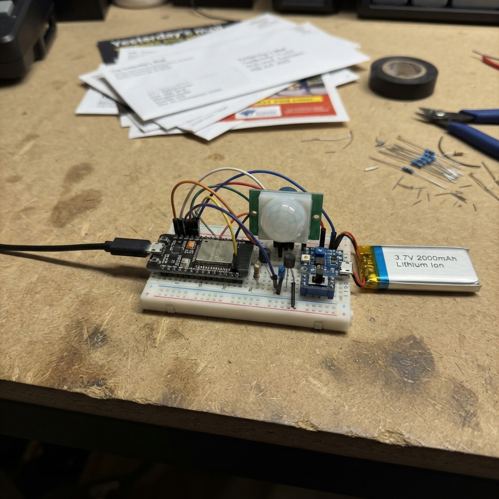
This Wi-Fi motion detector uses an ESP32 to detect movement via a PIR sensor and report it over wireless connectivity. The project combines a modified HC-SR501 motion sensor with battery-powered ESP32 operation, featuring a custom reset circuit that wakes the microcontroller only when motion is detected, minimizing power consumption for extended deployment.
The guide provides a complete wiring diagram, full parts list with sources, and step-by-step assembly instructions for building the detector on breadboard. Readers will learn how to integrate the TP4056 charging module for Li-Ion battery management, configure the HT7833A regulator for stable 3.3V operation, and implement the reset-pulse circuit that bridges the PIR sensor to the ESP32's reset pin. Firmware code is included to establish the wake-on-motion behavior and prepare for Wi-Fi connectivity.
Wiring diagram

Gather all the parts
Assemble it in 6 steps
1. Place the power parts
Put charger_1, power_switch_1, regulator_1, and the ESP-01 on the raster board. Your TP4056 is the protected six-pad version: it has IN+/IN− for 5 V charging, B+/B− for the cell, and OUT+/OUT− for the protected load. Connect charger_1 OUT+ to power_switch_1 COM (battery power), then connect switch A to regulator_1 VIN (switched battery power). Connect charger_1 OUT−, regulator_1 GND, and ESP-01 GND together (ground).
- Leave the TP4056 USB socket accessible for charging.
- Check the HT7833A-1 lead order from its marking or datasheet before soldering; TO-92 regulators do not all share the same order.
- Do not use B+ as the circuit supply: use OUT+ and OUT− so the TP4056 protection circuit remains between the cell and the load.
- Do not connect the Li-ion cell directly to ESP-01 VCC; a full cell is about 4.2 V and can damage the ESP-01.
2. Add the regulator capacitors
Connect regulator_input_cap_1 + to regulator_1 VIN (input smoothing) and its − lead to ground. Connect regulator_output_cap_1 + to regulator_1 VOUT (the 3.3 V rail) and its − lead to ground. Keep both capacitors close to the regulator.
- The striped side of an electrolytic capacitor is its − lead.
- Reversing an electrolytic capacitor can make it heat up or fail.
3. Wire the real ESP-01 header
Use the ESP-01’s actual eight header pins: VCC, RST, GND, GPIO0, TX/GPIO1, GPIO2, RX/GPIO3, and CH_PD. Connect VCC to the regulator 3.3 V rail (power), GND to ground (ground), and CH_PD directly to 3.3 V (enables the ESP). Connect reset_pullup_1 from 3.3 V to RST (keeps it out of reset). Connect gpio0_pullup_1 from 3.3 V to GPIO0 and gpio2_pullup_1 from 3.3 V to GPIO2 (normal boot settings). TX/GPIO1 and RX/GPIO3 are left available for programming. Fit esp_bulk_cap_1 and esp_bypass_cap_1 directly between VCC and GND beside the ESP-01: electrolytic + to VCC and − to GND; the ceramic part has no polarity.
- Keep the 470 µF capacitor and 0.1 µF ceramic capacitor physically close to ESP-01 VCC and GND.
- For ordinary running, GPIO0 and GPIO2 must not be connected to ground.
- Do not put 5 V on VCC, RST, CH_PD, GPIO0, GPIO1, GPIO2, or GPIO3. Every ESP-01 pin is a 3.3 V pin.
4. Wire the PIR sensor
Connect pir_1 VCC to the 3.3 V rail (power) and pir_1 GND to ground (ground). Connect pir_1 OUT to reset_series_resistor_1 A (motion signal), then connect reset_series_resistor_1 B to reset_pulse_cap_1 + (starts the short reset pulse).
- Set the HC-SR501 delay control to its shortest setting so it can report another movement sooner.
- This assumes your HC-SR501 has been modified and tested for a 3.3 V supply.
- Do not swap the PIR VCC and GND pins; swapped power can damage the sensor.
5. Make the reset pulse
Join reset_pulse_cap_1 −, reset_transistor_1 Base, base_pulldown_1 A, and the unmarked end of base_clamp_diode_1 into one point (reset-pulse control). Connect base_pulldown_1 B to ground (turns the transistor off after the short pulse). Connect the marked end of base_clamp_diode_1 to ground. Connect the 2N3904 Emitter to ground. Connect the 2N3904 Collector to the ESP-01 RST pin, at the same point as reset_pullup_1 B (reset signal). A new PIR detection briefly grounds RST, making the ESP-01 restart.
- The diode’s band marks its cathode; in this circuit the banded end goes to ground.
- Check the 2N3904’s pin order from the flat side before soldering.
- If the transistor collector and emitter are swapped, the ESP-01 may fail to reset or stay held in reset.
6. Connect and charge the battery
Connect battery_1 BAT+ to charger_1 B+ (battery positive) and battery_1 BAT− to charger_1 B− (battery negative). Charge only through the TP4056 USB input: USB 5 V reaches IN+ and USB ground reaches IN−. Before inserting the ESP-01, switch on and measure between the 3.3 V rail and ground; it should be close to 3.3 V.
- The PIR needs a short warm-up after power is first switched on.
- A reversed Li-ion cell can damage the charger and become dangerously hot. If any part gets hot, disconnect the battery immediately.
Review all connections
1. Connections between "battery_1" and "ESP32"
2. Connections between "charger_1" and "ESP32"
3. Connections between "power_switch_1" and "ESP32"
4. Connections between "regulator_1" and "ESP32"
5. Connections between "regulator_input_cap_1" and "ESP32"
6. Connections between "regulator_output_cap_1" and "ESP32"
7. Connections between "esp_bulk_cap_1" and "ESP32"
8. Connections between "esp_bypass_cap_1" and "ESP32"
9. Connections between "pir_1" and "ESP32"
10. Connections between "reset_series_resistor_1" and "ESP32"
11. Connections between "reset_pulse_cap_1" and "ESP32"
12. Connections between "base_pulldown_1" and "ESP32"
13. Connections between "base_clamp_diode_1" and "ESP32"
14. Connections between "reset_transistor_1" and "ESP32"
15. Connections between "reset_pullup_1" and "ESP32"
16. Connections between "gpio0_pullup_1" and "ESP32"
17. Connections between "gpio2_pullup_1" and "ESP32"
Deploy the firmware
#include <Arduino.h>

void setup() {
  // A PIR rising edge pulls RST low briefly and boots the ESP-01.
  // Future Wi-Fi reporting belongs here, before the sleep call.
  delay(25);
  ESP.deepSleep(0);
}

void loop() {
  // The ESP8266 does not reach this while deep sleep is active.
}
Remix this project
Make it yours in one click
Open a full copy of this project in your own Schematik workspace — diagram, code, parts, and assembly steps included. Swap the sensor, add features, or redesign the whole thing with AI. The author's original stays untouched.