Community project
Arduino Mage Npn 12v/24v 5v Io I2c Led
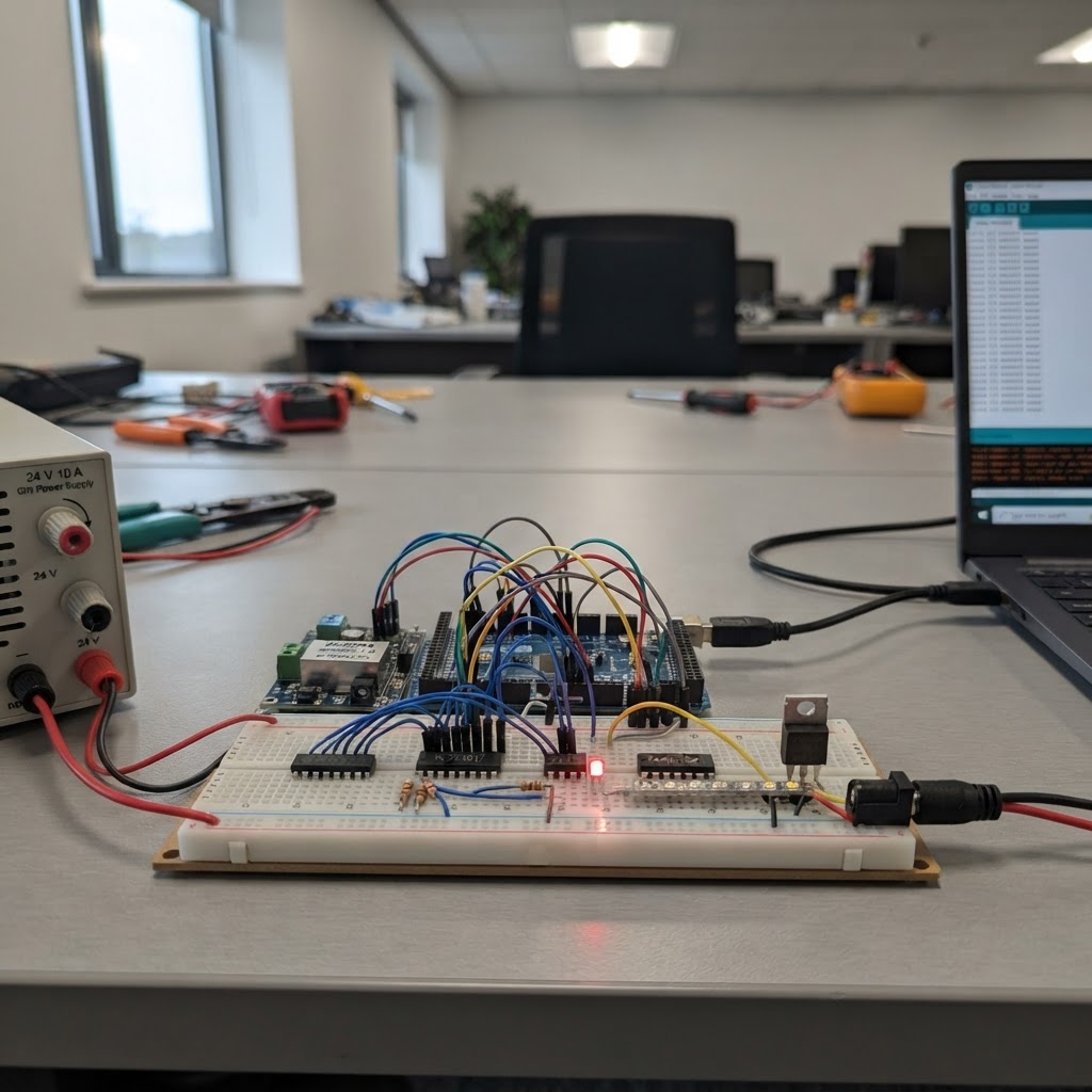
Generated with AIThis industrial I/O expansion board transforms an ESP32 into a robust 24 V control interface for factory automation, machinery, and process control applications. Built around an MCP23017 I2C GPIO expander with optocoupler-isolated inputs, MOSFET-driven outputs, and dual-voltage support (5 V logic, 12–24 V switching), the board safely bridges low-power microcontroller signals to high-power industrial loads while protecting against voltage spikes and noise.
The guide provides a complete wiring diagram, detailed parts list, and step-by-step assembly instructions covering power distribution, input conditioning, output switching stages, and I2C communication setup. Included firmware demonstrates debounced input sampling, safe output sequencing, and diagnostic LED feedback, enabling makers and technicians to deploy reliable automation logic without custom PCB design.
Wiring diagram

Interactive · read-only
Pan and zoom to explore the wiring. Remix the project to edit it in your own workspace.
Parts list
Bill of materials| Component | Qty | Notes |
|---|---|---|
| External 24 V 10 A DIN-rail DC power supply24 V DC, 10 A, external DIN-rail supply | 1 | An external enclosed supply that provides the board and field devices with 24 V DC. |
| RECOM R-78E5.0-1.0 switching regulator5 V, 1 A, SIP3 | 1 | A board-mounted switching regulator that converts the 12–24 V field supply to a regulated 5 V rail. |
| MCP23017 I2C GPIO expander ICTSSOP-28 | 1 | A 16-pin digital I/O chip that reads eight isolated inputs and controls eight output drivers over I2C. |
| PC817C optocouplerDIP-4, CTR grade C | 8 | An isolating light-coupler that safely transfers one 12–24 V NPN sensor signal to the 3.3 V logic side. |
| 74AHCT541 octal bufferTSSOP-20 | 1 | An eight-channel 5 V buffer that converts the MCP23017 3.3 V output signals into strong 5 V MOSFET gate-drive signals. |
| NVRGS055N06CL 60 V N-channel MOSFETSOT-23, 60 V, 70 mΩ max at VGS=4.5 V | 8 | A low-side power switch that connects one 24 V load to 0 V when its control signal is on. |
| 2.2 kΩ 0.5 W input resistor2.2 kΩ, 0.5 W, 1206 | 8 | A resistor that limits 12–24 V NPN sensor current before each optocoupler LED. |
| Red 0805 input status LEDRed, 0805 | 8 | A red light that shows when its NPN sensor input is being pulled to 0 V. |
| SS36 Schottky flyback diodeSS36, 3 A, 60 V, SMA | 8 | A diode that safely absorbs the voltage spike from one 24 V relay coil or solenoid when its output turns off. |
| Red 0805 output status LEDRed, 0805 | 8 | A red light that shows when its low-side MOSFET output is pulling the load terminal to 0 V. |
| 100 Ω MOSFET gate resistor100 Ω, 0603 | 8 | A resistor that limits each MOSFET gate charging pulse and reduces electrical noise. |
| 100 kΩ MOSFET gate pull-down resistor100 kΩ, 0603 | 8 | A resistor that keeps each output MOSFET safely off while the controller starts or is unplugged. |
| Logic pull-up and decoupling passive set2×4.7 kΩ 0603; 5×100 nF 0603; 2×10 µF 0805 | 1 | The I2C pull-up resistors and local ceramic capacitors that keep the logic supply and data signals stable. |
| 24 V input protection set10 A fuse, SS54 reverse diode, SMBJ33A TVS | 1 | A fuse, reverse-polarity diode and surge suppressor that protect the board from a miswired or noisy 24 V field supply. |
| Two-position 5.08 mm power terminal block2-position, 5.08 mm pitch, ≥10 A | 1 | The screw terminal where the 12–24 V field supply enters the circuit board. |
| Nine-position NPN sensor terminal block9-position, 5.08 mm pitch | 1 | The screw terminal block for eight NPN sensor signal wires and their shared 0 V return. |
| Nine-position output terminal block9-position, 5.08 mm pitch, ≥10 A | 1 | The screw terminal block for eight switched low-side load terminals and the shared protected +24 V feed. |
| Six-position 5 V GPIO terminal block6-position, 3.5 mm pitch | 1 | A screw terminal for four protected 5 V logic signals plus 5 V and ground. |
| Four-pin 3.3 V I2C header1×4, 2.54 mm | 1 | A keyed header for a low-voltage I2C device using 3.3 V logic. |
| 4.7 kΩ input LED resistor4.7 kΩ, 0.25 W, 1206 | 8 | A resistor that limits current through one 24 V input status LED. |
| 4.7 kΩ output LED resistor4.7 kΩ, 0.25 W, 1206 | 8 | A resistor that limits current through one 24 V output status LED. |
| 10 kΩ optocoupler pull-up resistor10 kΩ, 0603 | 8 | A resistor that makes one MCP23017 input read high when its optocoupler is off. |
| PCB mechanical hardware set2×7 XIAO female headers; 4×M3 mounting holes | 1 | Four mounting holes and the XIAO socket headers used to secure and plug in the controller. |
| Resettable output fuseMF-R110, 1.10 A hold PTC, radial | 8 | A protective fuse that limits fault current in one 24 V output channel. |
| 100 kΩ output-command pull-down resistor100 kΩ, 0603 | 8 | A resistor that keeps one output-command input low while the controller starts. |
| MCP23017 address and reset network3×0 Ω, 10 kΩ, 100 nF 0603 | 1 | Straps that set the expander to address 0x20 and keep its reset pin high. |
| 5 V GPIO direction-selection jumper1×3, 2.54 mm header plus shunt | 4 | A three-pin jumper that selects whether one translated 5 V signal is an input or an output. |
| SN74LVC1T45 5 V GPIO channel 1 translatorSN74LVC1T45, SC70-6 | 1 | A direction-controlled chip that safely translates the first XIAO signal between 3.3 V and 5 V. |
| SN74LVC1T45 5 V GPIO channel 2 translatorSN74LVC1T45, SC70-6 | 1 | A direction-controlled chip that safely translates the second XIAO signal between 3.3 V and 5 V. |
| SN74LVC1T45 5 V GPIO channel 3 translatorSN74LVC1T45, SC70-6 | 1 | A direction-controlled chip that safely translates the third XIAO signal between 3.3 V and 5 V. |
| SN74LVC1T45 5 V GPIO channel 4 translatorSN74LVC1T45, SC70-6 | 1 | A direction-controlled chip that safely translates the fourth XIAO signal between 3.3 V and 5 V. |
Assembly
8 steps准备外部 24 V 电源
把符合当地安全规范的封闭式 24 V 直流 DIN 导轨电源安装在机箱或导轨上。它的 +24V 线接到扩展板 J1 的 +24V,0V 线接到 J1 的 0V;这两根线为现场设备和扩展板供电。
- Tip: 先用万用表量 J1 两端,确认极性正确且电压在 12–24 V 范围内。
- ⚠ 交流市电只接外置、封闭且合规的 DIN 导轨电源;绝不能引入这块低压 PCB。
- ⚠ 把 +24V 与 0V 接反会使保护器件发热或损坏。
安装 XIAO 控制器
将 Seeed Studio XIAO ESP32S3 插入两排 1×7 母座,USB-C 接口朝向 PCB 外缘。确认每一排针脚都进入对应孔位,不要错位一列。
- Tip: 先只焊两个对角针脚,确认 USB-C 位置和板边方向正确后,再焊完其余针脚。
- ⚠ 焊接时不要让 5 V、3.3 V 或 GPIO 针脚之间产生焊锡桥接,否则可能损坏 XIAO。
装配输入区域
在 PCB 的 IN1–IN8 区域装入八颗 PC817C 光耦、每路 2.2 kΩ/0.5 W 输入电阻、4.7 kΩ LED 电阻和红色输入 LED。光耦缺口和 PCB 丝印缺口必须同向;LED 的短脚或外壳色带一侧是负端,按丝印方向安装。
- Tip: 每装完一路,用万用表检查该路没有把 +24V 短接到 0V。
- ⚠ 光耦和 LED 装反会导致该输入无指示或始终不工作。
- ⚠ 输入电阻必须使用 0.5 W、1206 或更大封装;普通小电阻可能在 24 V 现场侧过热。
装配输出区域
在 OUT1–OUT8 区域依照丝印安装八颗 MOSFET、每路 100 Ω 栅极电阻、100 kΩ 下拉电阻、MF-R110 自恢复保险丝、SS36 续流二极管、红色输出 LED 及其 4.7 kΩ 电阻。SS36 带条纹的一端必须朝向 +24V 丝印,另一端朝向对应 OUTn。
- Tip: 先检查每个 MOSFET 的封装方向,再焊接;SOT-23 的引脚很小,建议使用细焊锡和助焊剂。
- ⚠ 把续流二极管装反会在输出开启时直接短接 24 V,可能损坏保险丝、走线或电源。
- ⚠ 每路负载不得超过 1 A;八路同时工作时,外置电源、端子和铜箔必须承受总电流。
装配逻辑与电源区域
装入 MCP23017、74AHCT541、5 V 降压稳压器、逻辑上拉电阻、去耦电容和 24 V 保护器件。MCP23017 的 A0、A1、A2 接地,I²C 地址固定为 0x20;RESET 由上拉电阻接到 3.3 V。每颗 IC 的 100 nF 电容要紧贴其电源脚。
- Tip: 使用放大镜检查 TSSOP 引脚;相邻引脚间不应有焊锡连桥。
- ⚠ MCP23017 和 XIAO 只能使用 3.3 V 逻辑;不要把 5 V 接到 SDA、SCL 或 XIAO 的 GPIO。
连接传感器与执行器
每个三线 NPN 传感器:棕线接 +24V 公共端,蓝线接 0V 公共端,黑线接 IN1–IN8 中对应的一路。每个直流负载:正端接输出端子的 +24V_COM,负端接对应 OUT1–OUT8;该输出会把负端接到 0V 来启动负载。
- Tip: 先只接一个小型 24 V 指示灯或继电器线圈测试 OUT1,再逐路接入其余设备。
- ⚠ 感性负载必须使用本板对应通道的续流二极管;否则关断瞬间的尖峰可能损坏 MOSFET。
- ⚠ 不要把 NPN 传感器的黑色输出线直接接到 +24V。
选择并连接 5 V GPIO 与 I2C
J4 的 IO1–IO4 经过单通道电平转换器连接到 XIAO GPIO1–GPIO4;按每路 DIR 焊盘或跳线选择方向,输出模式把 DIR 接 3.3V,输入模式把 DIR 接 GND。J5 的四针顺序为 3V3、GND、SDA、SCL,SDA 接 GPIO5,SCL 接 GPIO6。
- Tip: 第一次使用 5 V GPIO 时,先选择输入模式并用万用表确认外部设备没有把电压送入错误端。
- ⚠ 不要把超过 5 V 的信号接到 J4;也不要把 24 V 现场信号接到 J4 或 J5。
第一次低风险上电
先不接执行器,仅连接 XIAO 的 USB-C 与外部 24 V。确认 5 V 稳压输出为约 5.0 V、XIAO 的 3.3 V 为约 3.3 V,并确认所有 OUT 灯在上电时熄灭。随后一次连接一个传感器和一个小负载验证 INn 动作时 OUTn 与两颗状态灯一起变化。
- Tip: 若某一路上电即导通,立即断开 24 V,检查该路 100 kΩ 栅极下拉、MOSFET 朝向和 74AHCT541 的 OE 接地。
- ⚠ 进行接线或更换负载前先断开 24 V 电源;带电插拔可能产生火花并损坏端子或输出器件。
Pin assignments
Board wiring reference| Pin | Connection | Type |
|---|---|---|
| EXT | field_psu_24v +24V → Two-position 5.08 mm power terminal block +V | power |
| EXT | field_psu_24v 0V → Two-position 5.08 mm power terminal block 0V | ground |
| EXT | tb_power +V → 24 V input protection set FIELD_IN | power |
| GND | tb_power 0V | ground |
| EXT | field_protection FIELD_PROTECTED → RECOM R-78E5.0-1.0 switching regulator VIN | power |
| GND | field_protection 0V | ground |
| VIN | pcb_reg_5v VIN | power |
| GND | pcb_reg_5v GND | ground |
| 5V | pcb_reg_5v VOUT | power |
| 3V3 | mcp23017_ic VDD | power |
| GND | mcp23017_ic VSS | ground |
| GPIO 5 | mcp23017_ic SDA | i2c |
| GPIO 6 | mcp23017_ic SCL | i2c |
| EXT | mcp23017_ic GPA0-GPA7 → PC817C optocoupler COLLECTOR | digital |
| EXT | mcp23017_ic GPB0-GPB7 → 74AHCT541 octal buffer A0-A7 | digital |
| EXT | opto_pc817c ANODE → 2.2 kΩ 0.5 W input resistor END2 | digital |
| EXT | opto_pc817c CATHODE → Nine-position NPN sensor terminal block IN1-IN8 | ground |
| EXT | opto_pc817c COLLECTOR → MCP23017 I2C GPIO expander IC GPA0-GPA7 | digital |
| GND | opto_pc817c EMITTER | ground |
| VIN | input_series_resistor END1 | power |
| EXT | input_series_resistor END2 → PC817C optocoupler ANODE | digital |
| VIN | input_indicator_led ANODE | power |
| EXT | input_indicator_led CATHODE → Nine-position NPN sensor terminal block IN1-IN8 | ground |
| GND | tb_inputs COM_0V | ground |
| EXT | tb_inputs IN1-IN8 → PC817C optocoupler CATHODE | digital |
| 5V | output_buffer VCC | power |
| GND | output_buffer GND | ground |
| EXT | output_buffer A0-A7 → MCP23017 I2C GPIO expander IC GPB0-GPB7 | digital |
| EXT | output_buffer Y0-Y7 → 100 Ω MOSFET gate resistor END1 | digital |
| GND | output_buffer OE1_OE2 | ground |
| EXT | gate_resistor END1 → 74AHCT541 octal buffer Y0-Y7 | digital |
| EXT | gate_resistor END2 → NVRGS055N06CL 60 V N-channel MOSFET GATE | digital |
| EXT | mosfet_gate_pulldown END1 → NVRGS055N06CL 60 V N-channel MOSFET GATE | digital |
| GND | mosfet_gate_pulldown END2 | ground |
| EXT | output_mosfet GATE → 100 Ω MOSFET gate resistor END2 | digital |
| EXT | output_mosfet DRAIN → Nine-position output terminal block OUT1-OUT8 | digital |
| GND | output_mosfet SOURCE | ground |
| EXT | output_flyback_diode ANODE → Nine-position output terminal block OUT1-OUT8 | ground |
| VIN | output_flyback_diode CATHODE | power |
| VIN | output_indicator_led ANODE | power |
| EXT | output_indicator_led CATHODE → Nine-position output terminal block OUT1-OUT8 | digital |
| VIN | tb_outputs +24V_COM | power |
| EXT | tb_outputs OUT1-OUT8 → NVRGS055N06CL 60 V N-channel MOSFET DRAIN | digital |
| 3V3 | hdr_i2c 3V3 | power |
| GND | hdr_i2c GND | ground |
| GPIO 5 | hdr_i2c SDA | i2c |
| GPIO 6 | hdr_i2c SCL | i2c |
| 3V3 | logic_passives 3V3 | power |
| 5V | logic_passives 5V | power |
| GND | logic_passives GND | ground |
| VIN | input_led_resistor END1 | power |
| EXT | input_led_resistor END2 → Red 0805 input status LED ANODE | digital |
| VIN | output_led_resistor END1 | power |
| EXT | output_led_resistor END2 → Red 0805 output status LED ANODE | digital |
| 3V3 | opto_pullup_resistor END1 | power |
| EXT | opto_pullup_resistor END2 → MCP23017 I2C GPIO expander IC GPA0-GPA7 | digital |
| GND | board_hardware GND_REFERENCE | ground |
| VIN | output_fuse IN | power |
| EXT | output_fuse OUT → Nine-position output terminal block +24V_COM | power |
| EXT | buffer_input_pulldown END1 → 74AHCT541 octal buffer A0-A7 | digital |
| GND | buffer_input_pulldown END2 | ground |
| GND | mcp_config A0_A1_A2 | ground |
| 3V3 | mcp_config RESET_PULLUP | power |
| GND | mcp_config DECOUPLING_GND | ground |
| 3V3 | gpio_dir_jumper OUTPUT_SELECT | power |
| GND | gpio_dir_jumper INPUT_SELECT | ground |
| EXT | gpio_dir_jumper COMMON → SN74LVC1T45 5 V GPIO channel 1 translator DIR | digital |
| 3V3 | gpio_translator_1 VCCA | power |
| 5V | gpio_translator_1 VCCB | power |
| GND | gpio_translator_1 GND | ground |
| GPIO 1 | gpio_translator_1 A | digital |
| EXT | gpio_translator_1 B → Six-position 5 V GPIO terminal block IO1-IO4 | digital |
| EXT | gpio_translator_1 DIR → 5 V GPIO direction-selection jumper COMMON | digital |
| 3V3 | gpio_translator_2 VCCA | power |
| 5V | gpio_translator_2 VCCB | power |
| GND | gpio_translator_2 GND | ground |
| GPIO 2 | gpio_translator_2 A | digital |
| EXT | gpio_translator_2 B → Six-position 5 V GPIO terminal block IO1-IO4 | digital |
| EXT | gpio_translator_2 DIR → 5 V GPIO direction-selection jumper COMMON | digital |
| 3V3 | gpio_translator_3 VCCA | power |
| 5V | gpio_translator_3 VCCB | power |
| GND | gpio_translator_3 GND | ground |
| GPIO 3 | gpio_translator_3 A | digital |
| EXT | gpio_translator_3 B → Six-position 5 V GPIO terminal block IO1-IO4 | digital |
| EXT | gpio_translator_3 DIR → 5 V GPIO direction-selection jumper COMMON | digital |
| 3V3 | gpio_translator_4 VCCA | power |
| 5V | gpio_translator_4 VCCB | power |
| GND | gpio_translator_4 GND | ground |
| GPIO 4 | gpio_translator_4 A | digital |
| EXT | gpio_translator_4 B → Six-position 5 V GPIO terminal block IO1-IO4 | digital |
| EXT | gpio_translator_4 DIR → 5 V GPIO direction-selection jumper COMMON | digital |
| 5V | tb_gpio5v +5V | power |
| GND | tb_gpio5v GND | ground |
Firmware
ESP32#include <Arduino.h>
#include <Wire.h>
#include <Adafruit_MCP23X17.h>
// Forward declarations
void setOutputsOff();
constexpr uint8_t I2C_SDA_PIN = 5;
constexpr uint8_t I2C_SCL_PIN = 6;
constexpr uint8_t GPIO5V_1_PIN = 1;
constexpr uint8_t GPIO5V_2_PIN = 2;
constexpr uint8_t GPIO5V_3_PIN = 3;
constexpr uint8_t GPIO5V_4_PIN = 4;
constexpr uint8_t MCP_ADDRESS = 0x20;
constexpr uint8_t CHANNEL_COUNT = 8;
constexpr uint32_t INPUT_STABLE_MS = 20;
Adafruit_MCP23X17 io;
bool stableInput[CHANNEL_COUNT] = {false};
bool sampledInput[CHANNEL_COUNT] = {false};
uint32_t lastChangeMs[CHANNEL_COUNT] = {0};
void setOutputsOff() {
for (uint8_t channel = 0; channel < CHANNEL_COUNT; ++channel) {
io.digitalWrite(channel + 8, LOW);
}
}
void setup() {
Serial.begin(115200);
Wire.begin(I2C_SDA_PIN, I2C_SCL_PIN);
pinMode(GPIO5V_1_PIN, INPUT);
pinMode(GPIO5V_2_PIN, INPUT);
pinMode(GPIO5V_3_PIN, INPUT);
pinMode(GPIO5V_4_PIN, INPUT);
if (!io.begin_I2C(MCP_ADDRESS, &Wire)) {
Serial.println("MCP23017 not found at 0x20; outputs remain unavailable.");
while (true) delay(1000);
}
for (uint8_t channel = 0; channel < CHANNEL_COUNT; ++channel) {
io.pinMode(channel, INPUT_PULLUP);
io.pinMode(channel + 8, OUTPUT);
}
setOutputsOff();
Serial.println("Industrial 8-in/8-out board ready.");
}
void loop() {
const uint32_t now = millis();
for (uint8_t channel = 0; channel < CHANNEL_COUNT; ++channel) {
const bool sensorOn = (io.digitalRead(channel) == LOW);
if (sensorOn != sampledInput[channel]) {
sampledInput[channel] = sensorOn;
lastChangeMs[channel] = now;
}
if (sampledInput[channel] != stableInput[channel] &&
now - lastChangeMs[channel] >= INPUT_STABLE_MS) {
stableInput[channel] = sampledInput[channel];
io.digitalWrite(channel + 8, stableInput[channel] ? HIGH : LOW);
Serial.printf("IN%u=%s, OUT%u=%s\n", channel + 1,
stableInput[channel] ? "ON" : "OFF", channel + 1,
stableInput[channel] ? "ON" : "OFF");
}
}
}“Deploy to device” opens this project in Schematik, where you can flash it to your board over USB.
Remix this project
Make it yours in one click
Open a full copy of this project in your own Schematik workspace — diagram, code, parts, and assembly steps included. Swap the sensor, add features, or redesign the whole thing with AI. The author's original stays untouched.