Community project
ESP32 Eight-Channel Relay Tester
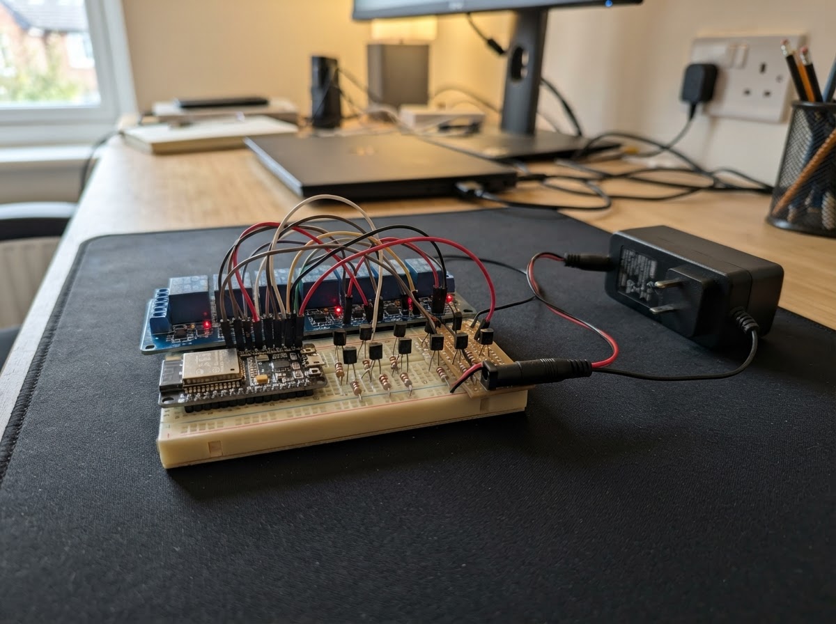
Generated with AIThis guide builds an eight-channel relay tester that validates each relay independently using an ESP32 microcontroller. The tester uses NPN transistors as low-side switches to control a JD-VCC relay module, allowing safe verification of relay operation without connecting any load circuits. Readers will receive a complete wiring diagram, parts list, and step-by-step assembly instructions.
The firmware cycles through each relay channel, energizing them one at a time and logging results to the serial monitor. This systematic approach makes it easy to identify any faulty relays or wiring issues before deploying the module in a real application. No external load or mains power is required—just the ESP32, relay module, transistors, resistors, and a regulated 5 V power supply.
Wiring diagram

Interactive · read-only
Pan and zoom to explore the wiring. Remix the project to edit it in your own workspace.
Parts list
Bill of materials| Component | Qty | Notes |
|---|---|---|
| 8-channel 5 V relay module with JD-VCC8 channels, 5 V | 1 | A ready-made board with eight relays that switches separate loads using its IN1 through IN8 control terminals. |
| Regulated 5 V, 2 A DC power supply5 V, 2 A | 1 | An external regulated supply that provides the 5 V power required by the relay board and its relay coils. |
| NPN Transistor (2N2222 / BC547)2N2222 | 1 | General-purpose NPN bipolar junction transistor (BJT) in TO-92 package. Used as a low-side switch to drive loads (e.g. buzzers) whose current exceeds ESP32 GPIO source capability (~12 mA). A ~1 kΩ base resistor is placed between the ESP32 GPIO and the transistor base. The collector connects to the load negative terminal (buzzer –), and the emitter connects to GND. When the GPIO goes HIGH (3.3 V), the transistor saturates and switches the load on. Compatible with both 2N2222/2N2222A and BC547/BC547B variants. Add a flyback diode (e.g. 1N4148) across inductive load terminals. |
| NPN Transistor (2N2222 / BC547)2N2222 | 1 | General-purpose NPN bipolar junction transistor (BJT) in TO-92 package. Used as a low-side switch to drive loads (e.g. buzzers) whose current exceeds ESP32 GPIO source capability (~12 mA). A ~1 kΩ base resistor is placed between the ESP32 GPIO and the transistor base. The collector connects to the load negative terminal (buzzer –), and the emitter connects to GND. When the GPIO goes HIGH (3.3 V), the transistor saturates and switches the load on. Compatible with both 2N2222/2N2222A and BC547/BC547B variants. Add a flyback diode (e.g. 1N4148) across inductive load terminals. |
| NPN Transistor (2N2222 / BC547)2N2222 | 1 | General-purpose NPN bipolar junction transistor (BJT) in TO-92 package. Used as a low-side switch to drive loads (e.g. buzzers) whose current exceeds ESP32 GPIO source capability (~12 mA). A ~1 kΩ base resistor is placed between the ESP32 GPIO and the transistor base. The collector connects to the load negative terminal (buzzer –), and the emitter connects to GND. When the GPIO goes HIGH (3.3 V), the transistor saturates and switches the load on. Compatible with both 2N2222/2N2222A and BC547/BC547B variants. Add a flyback diode (e.g. 1N4148) across inductive load terminals. |
| NPN Transistor (2N2222 / BC547)2N2222 | 1 | General-purpose NPN bipolar junction transistor (BJT) in TO-92 package. Used as a low-side switch to drive loads (e.g. buzzers) whose current exceeds ESP32 GPIO source capability (~12 mA). A ~1 kΩ base resistor is placed between the ESP32 GPIO and the transistor base. The collector connects to the load negative terminal (buzzer –), and the emitter connects to GND. When the GPIO goes HIGH (3.3 V), the transistor saturates and switches the load on. Compatible with both 2N2222/2N2222A and BC547/BC547B variants. Add a flyback diode (e.g. 1N4148) across inductive load terminals. |
| NPN Transistor (2N2222 / BC547)2N2222 | 1 | General-purpose NPN bipolar junction transistor (BJT) in TO-92 package. Used as a low-side switch to drive loads (e.g. buzzers) whose current exceeds ESP32 GPIO source capability (~12 mA). A ~1 kΩ base resistor is placed between the ESP32 GPIO and the transistor base. The collector connects to the load negative terminal (buzzer –), and the emitter connects to GND. When the GPIO goes HIGH (3.3 V), the transistor saturates and switches the load on. Compatible with both 2N2222/2N2222A and BC547/BC547B variants. Add a flyback diode (e.g. 1N4148) across inductive load terminals. |
| NPN Transistor (2N2222 / BC547)2N2222 | 1 | General-purpose NPN bipolar junction transistor (BJT) in TO-92 package. Used as a low-side switch to drive loads (e.g. buzzers) whose current exceeds ESP32 GPIO source capability (~12 mA). A ~1 kΩ base resistor is placed between the ESP32 GPIO and the transistor base. The collector connects to the load negative terminal (buzzer –), and the emitter connects to GND. When the GPIO goes HIGH (3.3 V), the transistor saturates and switches the load on. Compatible with both 2N2222/2N2222A and BC547/BC547B variants. Add a flyback diode (e.g. 1N4148) across inductive load terminals. |
| NPN Transistor (2N2222 / BC547)2N2222 | 1 | General-purpose NPN bipolar junction transistor (BJT) in TO-92 package. Used as a low-side switch to drive loads (e.g. buzzers) whose current exceeds ESP32 GPIO source capability (~12 mA). A ~1 kΩ base resistor is placed between the ESP32 GPIO and the transistor base. The collector connects to the load negative terminal (buzzer –), and the emitter connects to GND. When the GPIO goes HIGH (3.3 V), the transistor saturates and switches the load on. Compatible with both 2N2222/2N2222A and BC547/BC547B variants. Add a flyback diode (e.g. 1N4148) across inductive load terminals. |
| NPN Transistor (2N2222 / BC547)2N2222 | 1 | General-purpose NPN bipolar junction transistor (BJT) in TO-92 package. Used as a low-side switch to drive loads (e.g. buzzers) whose current exceeds ESP32 GPIO source capability (~12 mA). A ~1 kΩ base resistor is placed between the ESP32 GPIO and the transistor base. The collector connects to the load negative terminal (buzzer –), and the emitter connects to GND. When the GPIO goes HIGH (3.3 V), the transistor saturates and switches the load on. Compatible with both 2N2222/2N2222A and BC547/BC547B variants. Add a flyback diode (e.g. 1N4148) across inductive load terminals. |
| 1 kΩ resistor1 kΩ | 1 | A small resistor that limits current from ESP32 GPIO16 into the first transistor. |
| 1 kΩ resistor1 kΩ | 1 | A small resistor that limits current from ESP32 GPIO17 into the second transistor. |
| 1 kΩ resistor1 kΩ | 1 | A small resistor that limits current from ESP32 GPIO18 into the third transistor. |
| 1 kΩ resistor1 kΩ | 1 | A small resistor that limits current from ESP32 GPIO19 into the fourth transistor. |
| 1 kΩ resistor1 kΩ | 1 | A small resistor that limits current from ESP32 GPIO21 into the fifth transistor. |
| 1 kΩ resistor1 kΩ | 1 | A small resistor that limits current from ESP32 GPIO22 into the sixth transistor. |
| 1 kΩ resistor1 kΩ | 1 | A small resistor that limits current from ESP32 GPIO23 into the seventh transistor. |
| 1 kΩ resistor1 kΩ | 1 | A small resistor that limits current from ESP32 GPIO25 into the eighth transistor. |
Assembly
6 stepsLeave the relay screw terminals empty for the first test
Do not connect lamps, motors, wall power, or any other load to the relay screw terminals yet. This first test only checks that each relay clicks and its small channel light turns on.
- Tip: Place the relay module where you can see all eight small channel indicator lights.
- ⚠ Do not put wall power on the relay terminals while learning this test — a wiring mistake can cause electric shock, fire, or damage.
Place the eight resistors and transistors
Put the eight 1 kΩ resistors and eight 2N2222 transistors on a breadboard, leaving space between each channel. Keep each resistor with its matching transistor: R1 with Q1 through R8 with Q8. Before wiring, check the data sheet or package marking for your exact transistor’s flat-side pin order; different 2N2222 package styles can have different leg orders. Identify the base, collector, and emitter before applying power.
- Tip: Mark the transistor channels 1 through 8 with tape so the matching wires do not get mixed up.
- ⚠ Putting a transistor in with the wrong legs connected can prevent the relay from working and can stress the ESP32 output pin.
Wire the eight ESP32 control paths
With the ESP32 unplugged, wire GPIO16 → R1 → Q1 base (control), GPIO17 → R2 → Q2 base (control), GPIO18 → R3 → Q3 base (control), GPIO19 → R4 → Q4 base (control), GPIO21 → R5 → Q5 base (control), GPIO22 → R6 → Q6 base (control), GPIO23 → R7 → Q7 base (control), and GPIO25 → R8 → Q8 base (control). Each resistor must be in series between its ESP32 pin and transistor base; it limits the small control current.
- Tip: A resistor has no positive or negative end, so either leg can face the ESP32.
- ⚠ Do not connect an ESP32 GPIO straight to a transistor base without its 1 kΩ resistor — the resistor protects the ESP32 pin.
Connect the transistor outputs to the relay inputs
Connect Q1 collector → relay IN1 (signal), Q2 collector → IN2 (signal), Q3 collector → IN3 (signal), Q4 collector → IN4 (signal), Q5 collector → IN5 (signal), Q6 collector → IN6 (signal), Q7 collector → IN7 (signal), and Q8 collector → IN8 (signal). Connect every transistor emitter → ESP32 GND (ground). These transistors pull a relay input down to ground to turn its channel on.
- Tip: Keep the channel numbers matched from resistor to transistor to relay input; this makes the click sequence easy to verify.
- ⚠ Do not connect the relay’s 5 V VCC terminal to any ESP32 GPIO or to the ESP32 3V3 terminal — 5 V on an ESP32 signal pin can damage it.
Power the relay board from the external 5 V supply
Connect external supply +5V → relay VCC (relay input-side power) and external supply +5V → relay JD-VCC (relay coil power). Connect external supply GND → relay GND (ground) and external supply GND → ESP32 GND (shared ground). If the module has a VCC-to-JD-VCC jumper fitted, remove it before making these two separate +5 V connections. The ESP32 remains powered from its USB cable.
- Tip: Use a regulated 5 V supply rated for at least 2 A because all eight relays can be switched on together during the test.
- ⚠ Make sure +5 V and GND are not swapped — swapped power can damage the relay board. Do not feed the external 5 V supply into the ESP32 3V3 pin.
Run the relay click test
Plug the ESP32 into USB, then turn on the external 5 V relay supply. Press Schematik’s Deploy button. The program switches relay 1 through relay 8 on one at a time, then turns all eight on briefly before repeating.
- Tip: You should hear one click at a time and see the matching relay indicator light. The serial output names the channel currently being tested.
- ⚠ If a relay stays on unexpectedly, unplug the ESP32 USB cable and turn off the external 5 V supply before changing wires.
Pin assignments
Board wiring reference| Pin | Connection | Type |
|---|---|---|
| EXT | supply5v_1 +5V → 8-channel 5 V relay module with JD-VCC VCC | power |
| EXT | supply5v_1 +5V → 8-channel 5 V relay module with JD-VCC JD-VCC | power |
| GND | supply5v_1 GND | ground |
| GND | relay8_1 GND | ground |
| GND | q1 EMITTER | ground |
| GND | q2 EMITTER | ground |
| GND | q3 EMITTER | ground |
| GND | q4 EMITTER | ground |
| GND | q5 EMITTER | ground |
| GND | q6 EMITTER | ground |
| GND | q7 EMITTER | ground |
| GND | q8 EMITTER | ground |
| GPIO 16 | r1 END1 | digital |
| EXT | r1 END2 → NPN Transistor (2N2222 / BC547) BASE | digital |
| EXT | q1 COLLECTOR → 8-channel 5 V relay module with JD-VCC IN1 | digital |
| GPIO 17 | r2 END1 | digital |
| EXT | r2 END2 → NPN Transistor (2N2222 / BC547) BASE | digital |
| EXT | q2 COLLECTOR → 8-channel 5 V relay module with JD-VCC IN2 | digital |
| GPIO 18 | r3 END1 | digital |
| EXT | r3 END2 → NPN Transistor (2N2222 / BC547) BASE | digital |
| EXT | q3 COLLECTOR → 8-channel 5 V relay module with JD-VCC IN3 | digital |
| GPIO 19 | r4 END1 | digital |
| EXT | r4 END2 → NPN Transistor (2N2222 / BC547) BASE | digital |
| EXT | q4 COLLECTOR → 8-channel 5 V relay module with JD-VCC IN4 | digital |
| GPIO 21 | r5 END1 | digital |
| EXT | r5 END2 → NPN Transistor (2N2222 / BC547) BASE | digital |
| EXT | q5 COLLECTOR → 8-channel 5 V relay module with JD-VCC IN5 | digital |
| GPIO 22 | r6 END1 | digital |
| EXT | r6 END2 → NPN Transistor (2N2222 / BC547) BASE | digital |
| EXT | q6 COLLECTOR → 8-channel 5 V relay module with JD-VCC IN6 | digital |
| GPIO 23 | r7 END1 | digital |
| EXT | r7 END2 → NPN Transistor (2N2222 / BC547) BASE | digital |
| EXT | q7 COLLECTOR → 8-channel 5 V relay module with JD-VCC IN7 | digital |
| GPIO 25 | r8 END1 | digital |
| EXT | r8 END2 → NPN Transistor (2N2222 / BC547) BASE | digital |
| EXT | q8 COLLECTOR → 8-channel 5 V relay module with JD-VCC IN8 | digital |
Firmware
ESP32#include <Arduino.h>
// ESP32 eight-channel relay test through eight 2N2222 transistor switches.
// Each ESP32 HIGH passes through a 1 kΩ base resistor, turns its 2N2222 on,
// and pulls the matching active-low relay input to ground.
// Forward declarations
void setAllRelays(bool on);
const uint8_t RELAY_1_PIN = 16;
const uint8_t RELAY_2_PIN = 17;
const uint8_t RELAY_3_PIN = 18;
const uint8_t RELAY_4_PIN = 19;
const uint8_t RELAY_5_PIN = 21;
const uint8_t RELAY_6_PIN = 22;
const uint8_t RELAY_7_PIN = 23;
const uint8_t RELAY_8_PIN = 25;
const uint8_t relayPins[] = {
RELAY_1_PIN, RELAY_2_PIN, RELAY_3_PIN, RELAY_4_PIN,
RELAY_5_PIN, RELAY_6_PIN, RELAY_7_PIN, RELAY_8_PIN
};
const uint8_t RELAY_COUNT = sizeof(relayPins) / sizeof(relayPins[0]);
const unsigned long RELAY_ON_MS = 700;
const unsigned long GAP_MS = 300;
const unsigned long ALL_ON_MS = 1000;
const unsigned long ROUND_PAUSE_MS = 3000;
void setAllRelays(bool on) {
for (uint8_t i = 0; i < RELAY_COUNT; i++) {
digitalWrite(relayPins[i], on ? HIGH : LOW);
}
}
void setup() {
Serial.begin(115200);
for (uint8_t i = 0; i < RELAY_COUNT; i++) {
pinMode(relayPins[i], OUTPUT);
digitalWrite(relayPins[i], LOW); // Transistor off: relay input stays high, relay off.
}
Serial.println("8-channel relay test ready. No mains load is required for this test.");
}
void loop() {
for (uint8_t i = 0; i < RELAY_COUNT; i++) {
Serial.printf("Testing relay %u\n", i + 1);
digitalWrite(relayPins[i], HIGH);
delay(RELAY_ON_MS);
digitalWrite(relayPins[i], LOW);
delay(GAP_MS);
}
Serial.println("Testing all relays together");
setAllRelays(true);
delay(ALL_ON_MS);
setAllRelays(false);
Serial.println("Round complete; all relays off.");
delay(ROUND_PAUSE_MS);
}“Deploy to device” opens this project in Schematik, where you can flash it to your board over USB.
Remix this project
Make it yours in one click
Open a full copy of this project in your own Schematik workspace — diagram, code, parts, and assembly steps included. Swap the sensor, add features, or redesign the whole thing with AI. The author's original stays untouched.