Community project

Wi-Fi Door Sensor-vesm

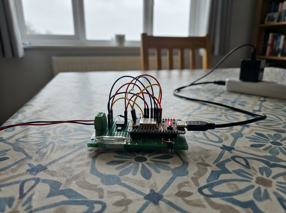
Photo of Wi-Fi Door Sensor-vesm
Generated with AI

Anuj Pagare

Published November 14, 2026

This Wi-Fi door sensor uses an ESP32 microcontroller to detect door open/closed states via a reed switch and broadcast the status over a local wireless network. The device connects to power through USB-C, regulates voltage with an AMS1117, and provides real-time door state monitoring accessible through a simple web interface.

The guide includes a complete wiring diagram, full parts list, pre-written firmware ready to flash, and step-by-step assembly instructions covering power input, ESP32 module installation, control button and LED connections, reed switch integration, and UART programming header setup.

Wiring diagram
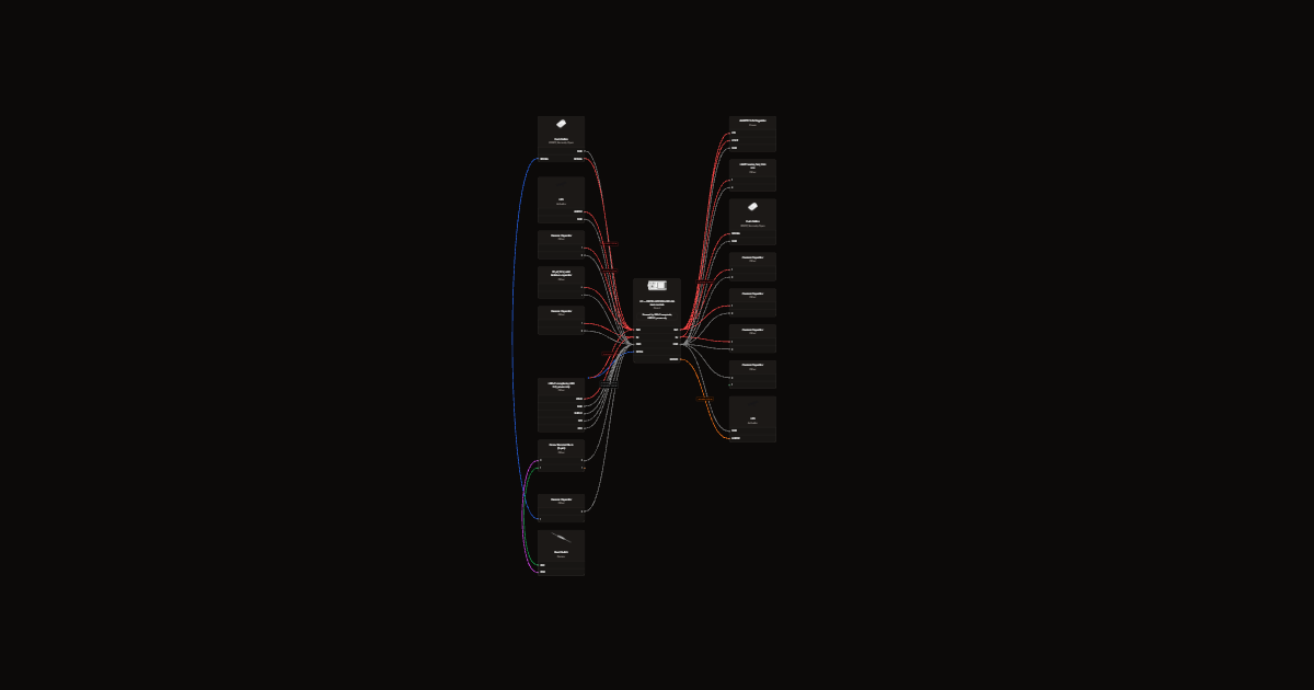
Wiring diagram for Wi-Fi Door Sensor-vesm
Loading diagram…

Gather all the parts

QtyComponent
1

USB-C receptacle, USB 2.0, power only

VBUS: A4/A9/B4/B9; GND: A1/A12/B1/B12; CC1 A5; CC2 B5. All data and SBU contacts unconnected. Bare connector, no built-in CC resistors.

1

AMS1117 3.3V Regulator

AMS1117-3.3, SOT-223: 1 GND, 2/tab VOUT, 3 VIN

Linear LDO regulator, 5 V (or higher) in -> 3.3 V out, 1 A max. Used to drop a 5 V supply down to 3.3 V for ESP32 / Pico when no on-board regulator is available.

1

Screw Terminal Block (2-pin)

2-pin 5.08 mm reed terminal

Two-position PCB screw terminal block with 5.0 or 5.08 mm pitch for clamping wires to a circuit board. Each position takes a stripped wire of roughly 22 to 14 AWG and connects it to one through-hole pad, and blocks interlock side by side for more positions.

1

UART header, 1x4, 2.54 mm

Pin order: 1 3V3 reference, 2 ESP TX, 3 ESP RX, 4 GND. 3.3 V logic only. Do not connect adapter power while USB powers board.

1

Push Button

RESET, normally open

Momentary push button switch

1

Push Button

BOOT, normally open

Momentary push button switch

1

LED

green power LED

Standard 3mm/5mm through-hole LED. A current-limiting series resistor is added automatically.

1

LED

red door-open status LED

Standard 3mm/5mm through-hole LED. A current-limiting series resistor is added automatically.

1

Reed Switch

external normally-open magnetic contact; closes with magnet

Glass-encapsulated magnetic reed switch -- contacts close in the presence of a magnetic field. Standard door/window sensor for alarms. Wire as a digital input with internal pull-up; debounce in firmware.

1

Resistor

5.1 kΩ ±1%, 0.125 W

Through-hole resistor (current-limiting in series with an LED)

1

Resistor

5.1 kΩ ±1%, 0.125 W

Through-hole resistor (current-limiting in series with an LED)

1

Resistor

10 kΩ ±1%, 0.125 W

Through-hole resistor (current-limiting in series with an LED)

1

Resistor

10 kΩ ±1%, 0.125 W

Through-hole resistor (current-limiting in series with an LED)

1

Resistor

10 kΩ ±1%, 0.125 W

Through-hole resistor (current-limiting in series with an LED)

1

Resistor

1 kΩ ±1%, 0.125 W

Through-hole resistor (current-limiting in series with an LED)

1

Resistor

1 kΩ ±1%, 0.125 W

Through-hole resistor (current-limiting in series with an LED)

1

Resistor

1 kΩ ±1%, 0.125 W

Through-hole resistor (current-limiting in series with an LED)

1

Ceramic Capacitor

4.7 µF, 16 V, X7R

Through-hole ceramic capacitor bought by value, such as 22 pF, 10 nF or 100 nF (0.1 µF). It is non-polarised, so either lead can go to either net. Its most common job is decoupling: a 100 nF capacitor between an IC's supply pin and ground, placed as close to the chip as possible.

1

Ceramic Capacitor

100 nF, 16 V, X7R

Through-hole ceramic capacitor bought by value, such as 22 pF, 10 nF or 100 nF (0.1 µF). It is non-polarised, so either lead can go to either net. Its most common job is decoupling: a 100 nF capacitor between an IC's supply pin and ground, placed as close to the chip as possible.

1

Ceramic Capacitor

100 nF, 16 V, X7R

Through-hole ceramic capacitor bought by value, such as 22 pF, 10 nF or 100 nF (0.1 µF). It is non-polarised, so either lead can go to either net. Its most common job is decoupling: a 100 nF capacitor between an IC's supply pin and ground, placed as close to the chip as possible.

1

Ceramic Capacitor

10 µF, 16 V, X7R (effective ≥10 µF at 3.3 V)

Through-hole ceramic capacitor bought by value, such as 22 pF, 10 nF or 100 nF (0.1 µF). It is non-polarised, so either lead can go to either net. Its most common job is decoupling: a 100 nF capacitor between an IC's supply pin and ground, placed as close to the chip as possible.

1

Ceramic Capacitor

100 nF, 16 V, X7R

Through-hole ceramic capacitor bought by value, such as 22 pF, 10 nF or 100 nF (0.1 µF). It is non-polarised, so either lead can go to either net. Its most common job is decoupling: a 100 nF capacitor between an IC's supply pin and ground, placed as close to the chip as possible.

1

Ceramic Capacitor

1 µF, 16 V, X7R

Through-hole ceramic capacitor bought by value, such as 22 pF, 10 nF or 100 nF (0.1 µF). It is non-polarised, so either lead can go to either net. Its most common job is decoupling: a 100 nF capacitor between an IC's supply pin and ground, placed as close to the chip as possible.

1

Ceramic Capacitor

100 nF, 16 V, X7R

Through-hole ceramic capacitor bought by value, such as 22 pF, 10 nF or 100 nF (0.1 µF). It is non-polarised, so either lead can go to either net. Its most common job is decoupling: a 100 nF capacitor between an IC's supply pin and ground, placed as close to the chip as possible.

1

22 µF, 16 V, solid tantalum capacitor

Polarized output stability capacitor; use genuine AMS1117 with its specified 22 µF tantalum output capacitor, not ceramic-only substitution.

Assemble it in 5 steps

1. Assemble the power input

Fit J1 and its separate R1/R2 CC pull-downs. Connect all VBUS contacts to +5V, all ground contacts and shell tabs to GND. Leave data/SBU pins unconnected. Fit U1, C1, C2, C3 and C4. U1 SOT-223 pin 1 is GND, pin 2 and tab are 3V3, pin 3 is +5V.

  • C3 is polarized: positive to 3V3. U1 tab is NOT ground. Use a dedicated 5 V USB supply rated at least 1 A; CC resistors do not negotiate USB PD or detect available current.

2. Fit the ESP32 module and bypass capacitors

Fit U2 ESP32-WROOM-32E-N4 to a PCB footprint. Pin 2 goes to 3V3. Ground pins 1, 15, 38 and exposed pad 39. Place C5 and C6 at pin 2. Leave NC pins 17–22 and 32 unconnected, and leave unused GPIOs unconnected. Keep all copper, traces and components out of the antenna keepout on every layer.

  • The module already contains its crystal, flash and RF matching. Give U1 a large 3V3 copper heat-spreading area; dissipation reaches about 0.85 W at 500 mA. Check its temperature under Wi-Fi load.

3. Fit reset and boot controls

R3 pulls EN (U2 pin 3) to 3V3; C7 delays EN at startup. SW1 grounds EN when pressed. R4 pulls GPIO0 (pin 25) to 3V3; SW2 grounds it for programming. Leave GPIO2 and GPIO12 unconnected so their internal boot pull-downs are not overridden.

4. Connect the door contact and LEDs

J2 pin 1 connects through R6 to GPIO4 (U2 pin 26). R5 pulls GPIO4 high; C8 filters it to ground. J2 pin 2 is ground. Connect the reed contact between the two terminals. D1 is powered through R7 from 3V3. GPIO25 (pin 10) drives D2 through R8. Both LED cathodes go to ground.

  • Use short indoor reed-switch wiring. This input has no surge protection for long outdoor cables.

5. Check power and connect programming header

Before fitting power, check for shorts. Measure 3V3 before programming. J3 pins are 1=3V3 reference, 2=ESP TX GPIO1 (U2 pin 35), 3=ESP RX GPIO3 (pin 34), 4=GND. Adapter RX goes to J3 pin 2 and adapter TX to pin 3. Use only 3.3 V UART logic.

  • Hold BOOT, press and release RESET, then release BOOT to enter download mode. Reset again after programming. The four-pin header has no automatic reset signals.
  • When USB powers the board, leave the adapter power lead disconnected. J3 3V3 is a reference/output, not a second supply input. Never connect 5 V TTL or RS-232 signals.

Review all connections

1. Connections between "R1" and "ESP32"

FunctionR1ESP32
digitalP1 → USB-C receptacle, USB 2.0, power only CC1EXT
groundP2GND

2. Connections between "R2" and "ESP32"

FunctionR2ESP32
digitalP1 → USB-C receptacle, USB 2.0, power only CC2EXT
groundP2GND

3. Connections between "R3" and "ESP32"

FunctionR3ESP32
powerP13V3
digitalP2 → Push Button SIGNALEXT

4. Connections between "R4" and "ESP32"

FunctionR4ESP32
powerP13V3
digitalP2 → Push Button SIGNALEXT

5. Connections between "R5" and "ESP32"

FunctionR5ESP32
powerP13V3
digitalP2 → Resistor P2EXT

6. Connections between "R6" and "ESP32"

FunctionR6ESP32
digitalP1 → Screw Terminal Block (2-pin) 1EXT
digitalP2GPIO 4

7. Connections between "R7" and "ESP32"

FunctionR7ESP32
powerP13V3
digitalP2 → LED ANODEEXT

8. Connections between "R8" and "ESP32"

FunctionR8ESP32
digitalP1GPIO 25
digitalP2 → LED ANODEEXT

9. Connections between "C1" and "ESP32"

FunctionC1ESP32
power15V
ground2GND

10. Connections between "C2" and "ESP32"

FunctionC2ESP32
power15V
ground2GND

11. Connections between "C4" and "ESP32"

FunctionC4ESP32
power13V3
ground2GND

12. Connections between "C5" and "ESP32"

FunctionC5ESP32
power13V3
ground2GND

13. Connections between "C6" and "ESP32"

FunctionC6ESP32
power13V3
ground2GND

14. Connections between "C7" and "ESP32"

FunctionC7ESP32
digital1 → Push Button SIGNALEXT
ground2GND

15. Connections between "C8" and "ESP32"

FunctionC8ESP32
digital1 → Resistor P2EXT
ground2GND

16. Connections between "C3" and "ESP32"

FunctionC3ESP32
power+3V3
ground-GND

17. Connections between "J1" and "ESP32"

FunctionJ1ESP32
powerVBUS5V
groundGNDGND
groundSHIELDGND

18. Connections between "U1" and "ESP32"

FunctionU1ESP32
powerVIN5V
powerVOUT3V3
groundGNDGND

19. Connections between "SW1" and "ESP32"

FunctionSW1ESP32
digitalSIGNAL → Module EN reset padEXT
groundGNDGND

20. Connections between "SW2" and "ESP32"

FunctionSW2ESP32
digitalSIGNAL → Module IO0 download strap padEXT
groundGNDGND

21. Connections between "J2" and "ESP32"

FunctionJ2ESP32
ground2GND

22. Connections between "REED1" and "ESP32"

FunctionREED1ESP32
dataPIN1 → Screw Terminal Block (2-pin) 1EXT
groundPIN2 → Screw Terminal Block (2-pin) 2EXT

23. Connections between "D1" and "ESP32"

FunctionD1ESP32
groundGNDGND

24. Connections between "D2" and "ESP32"

FunctionD2ESP32
groundGNDGND

25. Connections between "J3" and "ESP32"

FunctionJ3ESP32
power13V3
data2 → Module TXD0 padEXT
data3 → Module RXD0 padEXT
ground4GND

Deploy the firmware

#include <Arduino.h>
#include <WiFi.h>
#include <WebServer.h>
WebServer server(80);
constexpr int REED_PIN=4, STATUS_LED_PIN=25;
bool stableOpen=true, lastRaw=true;
uint32_t changedAt=0;
void setup(){
  pinMode(REED_PIN,INPUT); pinMode(STATUS_LED_PIN,OUTPUT);
  Serial.begin(115200);
  stableOpen=lastRaw=digitalRead(REED_PIN); digitalWrite(STATUS_LED_PIN,stableOpen);
  WiFi.mode(WIFI_AP);
  WiFi.softAP("DoorSensor", "DoorSensor32!");
  server.on("/", [](){server.send(200,"text/plain",stableOpen?"Door OPEN\n":"Door CLOSED\n");});
  server.begin();
  Serial.println("Connect to DoorSensor; password DoorSensor32!; visit http://192.168.4.1/");
}
void loop(){
 server.handleClient();
 bool raw=digitalRead(REED_PIN);
 if(raw!=lastRaw){lastRaw=raw;changedAt=millis();}
 if(raw!=stableOpen && millis()-changedAt>=40){stableOpen=raw;digitalWrite(STATUS_LED_PIN,stableOpen);Serial.println(stableOpen?"OPEN":"CLOSED");}
}

Remix this project

Make it yours in one click

Open a full copy of this project in your own Schematik workspace, diagram, code, parts, and assembly steps included. Swap the sensor, add features, or redesign the whole thing with AI. The author's original stays untouched.
Open in Schematik