Community project
ESP32 Noise Signal Generator
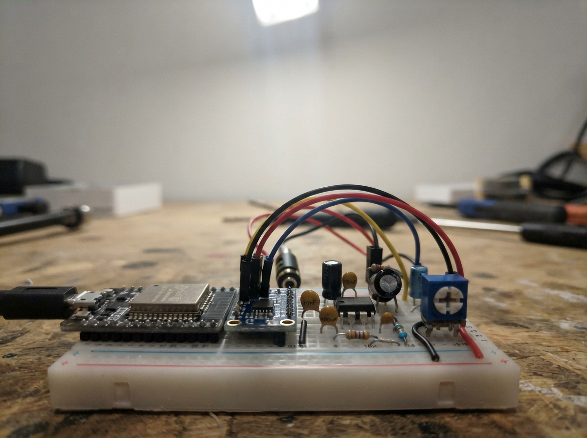
This project builds a low-level noise signal generator using an ESP32 microcontroller, a MCP4725 digital-to-analog converter, and an LM358 operational amplifier buffer. The generator produces white noise, pinkish noise, and burst modes at 4 kHz sample rate, with amplitude control via a front-panel potentiometer. Output is protected and suitable for audio testing, signal processing experiments, and laboratory work.
The guide provides a complete wiring diagram, full parts list with values, Arduino firmware with multiple noise algorithms, and step-by-step assembly instructions. Builders will learn how to interface the ESP32 with I2C DAC modules, design simple analog filters and buffers, implement real-time signal generation on microcontroller hardware, and add user controls for live parameter adjustment.
Wiring diagram

Gather all the parts
Assemble it in 6 steps
1. Place the board and make power rails
Push the ESP32 DevKit V1 across the centre gap of the breadboard. Use the board’s 3V3 pin as the 3.3 V rail, its 5V/VIN pin as the 5 V rail, and join every ground connection to one common GND rail. Power the board only through its USB connector.
- Keep the analogue parts close together at one end of the breadboard; keep the USB cable and long digital wires away from the output node.
- Do not connect a separate 5 V supply while USB is powering the ESP32; two supplies connected together can damage the board or computer USB port.
2. Wire the MCP4725 converter
Connect MCP4725 VCC to ESP32 3V3 (power), GND to ESP32 GND (ground), SDA to GPIO21 (data), SCL to GPIO22 (clock), and ADDR to GND (address select). Put c_dac_decouple_1, 100 nF ceramic, directly between the MCP4725 VCC and GND pins. Put c_dac_bulk_1, 10 µF electrolytic, across the same rails: its positive lead goes to 3V3 and its striped negative lead goes to GND.
- The MCP4725 OUT pin is the analogue signal; do not confuse it with the address pin.
- Keep the MCP4725 on 3.3 V, not 5 V: many low-cost modules pull SDA and SCL up to their own supply, and 5 V on ESP32 pins can damage the ESP32.
3. Build the filter and LM358 buffer
Connect MCP4725 OUT to one end of r_filter_1, 10 kΩ. Join its other end to c_filter_1 and to LM358 pin 3, IN+ A. Connect the other c_filter_1 lead to GND. For the LM358 follower, connect pin 1 OUT A directly to pin 2 IN− A. Connect pin 8 VCC to 5 V (power) and pin 4 GND to GND (ground). Put c_opamp_decouple_1, 100 nF ceramic, and c_opamp_bulk_1, 10 µF electrolytic, from pin 8/5 V to pin 4/GND; the striped lead of the electrolytic goes to GND. Disable the unused half: join pin 7 OUT B to pin 6 IN− B, and connect pin 5 IN+ B to GND.
- If using a bare DIP-8 IC, find the notch first: pin 1 is the pin immediately to the left of the notch when viewed from above.
- Do not reverse the 10 µF electrolytic capacitors; a reversed electrolytic can heat up and fail.
4. Add the protected low-level output
Connect LM358 pin 1 to the positive lead of c_output_1, 10 µF. Connect the capacitor’s striped negative lead to one end of r_output_protect_1, 100 Ω. Connect the other end of that resistor to output_terminal_1 SIG (signal). Connect r_load_1, 10 kΩ, from SIG to GND, and connect the terminal GND pin to the common GND rail.
- Use a short wire from SIG to the oscilloscope probe tip and connect the probe ground clip only to the output GND terminal.
- This is a low-level laboratory output only; do not connect it to an antenna, a transmitter input, mains equipment, or a low-impedance load such as a speaker.
5. Wire the level control
Connect one outside leg of amplitude_pot_1 to 3V3 (power), its other outside leg to GND (ground), and its middle leg to GPIO34 (signal). Put c_pot_smooth_1, 100 nF ceramic, between the middle leg and GND.
- If turning the knob clockwise reduces the level, swap the two outside potentiometer wires; the middle wire stays on GPIO34.
- The potentiometer must use 3.3 V, not 5 V, because GPIO34 must never receive more than 3.3 V.
6. Inspect before first power-up
With USB unplugged, check that the 3V3 rail does not short to GND and that the 5 V rail does not short to GND. Check that the MCP4725 has 3.3 V, while the LM358 has 5 V. Then plug in USB power and use Schematik’s Deploy button to compile and flash the firmware.
- Start with the amplitude knob near its lowest setting, then increase it while watching the output.
- If a module becomes hot, unplug USB immediately and recheck VCC, GND, and every electrolytic capacitor direction.
Review all connections
1. Connections between "dac_1" and "ESP32"
2. Connections between "r_filter_1" and "ESP32"
3. Connections between "c_filter_1" and "ESP32"
4. Connections between "opamp_1" and "ESP32"
5. Connections between "c_dac_decouple_1" and "ESP32"
6. Connections between "c_dac_bulk_1" and "ESP32"
7. Connections between "c_opamp_decouple_1" and "ESP32"
8. Connections between "c_opamp_bulk_1" and "ESP32"
9. Connections between "c_output_1" and "ESP32"
10. Connections between "r_output_protect_1" and "ESP32"
11. Connections between "r_load_1" and "ESP32"
12. Connections between "output_terminal_1" and "ESP32"
13. Connections between "amplitude_pot_1" and "ESP32"
14. Connections between "c_pot_smooth_1" and "ESP32"
Deploy the firmware
#include <Arduino.h>
#include <Wire.h>
#include <Adafruit_MCP4725.h>

// Low-level laboratory noise source: no RF power stage and no antenna.

// Hoisted type definitions
enum NoiseMode : uint8_t { WHITE = 0, PINKISH = 1, BURST = 2 };


// Forward declarations
uint32_t nextRandom();
int16_t makeSample();
void IRAM_ATTR onSampleTimer();
void dacWriterTask(void *);
void printStatus();
void processCommand(String command);

constexpr uint8_t I2C_SDA_PIN = 21;
constexpr uint8_t I2C_SCL_PIN = 22;
constexpr uint8_t AMPLITUDE_POT_PIN = 34;
constexpr uint8_t MCP4725_ADDRESS = 0x60;
constexpr uint32_t SAMPLE_RATE_HZ = 4000;
constexpr uint32_t TIMER_TICK_US = 1000000UL / SAMPLE_RATE_HZ;

Adafruit_MCP4725 dac;
hw_timer_t *sampleTimer = nullptr;
TaskHandle_t dacTaskHandle = nullptr;

portMUX_TYPE timerMux = portMUX_INITIALIZER_UNLOCKED;
volatile bool generatorEnabled = true;
volatile bool timerTick = false;


volatile NoiseMode mode = WHITE;
volatile uint16_t manualAmplitude = 0;  // 0 means use the front-panel potentiometer.
uint32_t rngState = 0xA5C35A17UL;
int32_t pinkState = 0;
uint32_t lastControlReadMs = 0;
uint16_t potAmplitude = 3072;

uint32_t nextRandom() {
  rngState ^= rngState << 13;
  rngState ^= rngState >> 17;
  rngState ^= rngState << 5;
  return rngState;
}

int16_t makeSample() {
  int16_t white = static_cast<int16_t>((nextRandom() >> 16) & 0xFFFF) - 32768;

  if (mode == WHITE) return white;

  if (mode == PINKISH) {
    // One-pole low-pass of white noise: visibly more low-frequency content.
    pinkState += (static_cast<int32_t>(white) - pinkState) >> 3;
    return static_cast<int16_t>(constrain(pinkState, -32768L, 32767L));
  }

  // A repeating 250 ms ON / 250 ms OFF noise burst for trigger tests.
  uint32_t phase = (millis() / 250UL) & 1U;
  return phase == 0 ? white : 0;
}

void IRAM_ATTR onSampleTimer() {
  BaseType_t higherPriorityTaskWoken = pdFALSE;
  timerTick = true;
  vTaskNotifyGiveFromISR(dacTaskHandle, &higherPriorityTaskWoken);
  if (higherPriorityTaskWoken) portYIELD_FROM_ISR();
}

void dacWriterTask(void *) {
  for (;;) {
    ulTaskNotifyTake(pdTRUE, portMAX_DELAY);
    if (!generatorEnabled) {
      dac.setVoltage(2048, false);
      continue;
    }

    uint16_t amplitude = manualAmplitude ? manualAmplitude : potAmplitude;
    int32_t signedValue = makeSample();
    int32_t centeredCode = 2048 + ((signedValue * amplitude) >> 16);
    uint16_t code = static_cast<uint16_t>(constrain(centeredCode, 0L, 4095L));
    dac.setVoltage(code, false);
  }
}

void printStatus() {
  const char *names[] = {"white", "pinkish", "burst"};
  uint16_t amplitude = manualAmplitude ? manualAmplitude : potAmplitude;
  Serial.println();
  Serial.println("Noise generator status");
  Serial.printf("mode: %s\n", names[mode]);
  Serial.printf("sample rate: %lu Hz\n", static_cast<unsigned long>(SAMPLE_RATE_HZ));
  Serial.printf("amplitude: %u / 4095 (%s)\n", amplitude,
                manualAmplitude ? "Serial setting" : "front-panel potentiometer");
  Serial.printf("output: %s\n", generatorEnabled ? "enabled" : "muted at DAC midpoint");
  Serial.println("Commands: help | status | mode white|pink|burst | amp 0..4095 | pot | on | off");
}

void processCommand(String command) {
  command.trim();
  command.toLowerCase();
  if (command == "help") {
    Serial.println("help | status | mode white|pink|burst | amp 0..4095 | pot | on | off");
  } else if (command == "status") {
    printStatus();
  } else if (command == "mode white") {
    mode = WHITE; Serial.println("Mode set to white.");
  } else if (command == "mode pink") {
    mode = PINKISH; Serial.println("Mode set to pinkish.");
  } else if (command == "mode burst") {
    mode = BURST; Serial.println("Mode set to burst.");
  } else if (command == "pot") {
    manualAmplitude = 0; Serial.println("Amplitude now follows the potentiometer.");
  } else if (command == "on") {
    generatorEnabled = true; Serial.println("Output enabled.");
  } else if (command == "off") {
    generatorEnabled = false; Serial.println("Output muted.");
  } else if (command.startsWith("amp ")) {
    long value = command.substring(4).toInt();
    if (value >= 0 && value <= 4095) {
      manualAmplitude = static_cast<uint16_t>(value);
      Serial.printf("Amplitude set to %ld / 4095.\n", value);
    } else {
      Serial.println("Amplitude must be from 0 to 4095.");
    }
  } else if (command.length()) {
    Serial.println("Unknown command. Type help.");
  }
}

void setup() {
  Serial.begin(115200);
  delay(300);
  analogReadResolution(12);
  Wire.begin(I2C_SDA_PIN, I2C_SCL_PIN, 400000);

  if (!dac.begin(MCP4725_ADDRESS, &Wire)) {
    Serial.println("MCP4725 was not found at I2C address 0x60. Check 3.3V, GND, SDA and SCL.");
    while (true) delay(1000);
  }
  dac.setVoltage(2048, false);

  xTaskCreatePinnedToCore(dacWriterTask, "dacWriter", 4096, nullptr, 3, &dacTaskHandle, 1);
  sampleTimer = timerBegin(0, 80, true);  // 80 MHz / 80 = 1 MHz timer tick.
  timerAttachInterrupt(sampleTimer, &onSampleTimer, true);
  timerAlarmWrite(sampleTimer, TIMER_TICK_US, true);
  timerAlarmEnable(sampleTimer);

  Serial.println("ESP32 low-level noise generator ready.");
  printStatus();
}

void loop() {
  if (millis() - lastControlReadMs >= 40) {
    lastControlReadMs = millis();
    // ADC1/GPIO34 is safe while Wi-Fi remains unused; average four readings.
    uint32_t total = 0;
    for (uint8_t i = 0; i < 4; ++i) total += analogRead(AMPLITUDE_POT_PIN);
    potAmplitude = static_cast<uint16_t>(total / 4);
  }

  if (Serial.available()) {
    String command = Serial.readStringUntil('\n');
    processCommand(command);
  }
}
Remix this project
Make it yours in one click
Open a full copy of this project in your own Schematik workspace — diagram, code, parts, and assembly steps included. Swap the sensor, add features, or redesign the whole thing with AI. The author's original stays untouched.